Inquire: Call 0086-755-23203480, or reach out via the form below/your sales contact to discuss our design, manufacturing, and assembly capabilities.
Quote: Email your PCB files to Sales@pcbsync.com (Preferred for large files) or submit online. We will contact you promptly. Please ensure your email is correct.
Notes: For PCB fabrication, we require PCB design file in Gerber RS-274X format (most preferred), *.PCB/DDB (Protel, inform your program version) format or *.BRD (Eagle) format. For PCB assembly, we require PCB design file in above mentioned format, drilling file and BOM. Click to download BOM template To avoid file missing, please include all files into one folder and compress it into .zip or .rar format.
After designing embedded systems that push data rates to their limits—from high-resolution TFT displays refreshing at 60fps to SD cards recording sensor telemetry at megabit speeds—I’ve learned that mastering Arduino SPI communication separates basic microcontroller projects from professional-grade systems. SPI represents the fastest synchronous serial protocol available on Arduino platforms, capable of clock speeds exceeding 10 MHz on many boards. Understanding when to choose SPI over I2C or UART, how to configure the four clock modes correctly, and managing multiple slave devices efficiently transforms your projects from proof-of-concept prototypes into production-ready designs.
Serial Peripheral Interface, developed by Motorola in the mid-1980s, remains the de facto standard for high-speed short-distance communication between microcontrollers and peripheral devices. The protocol employs a master-slave architecture where one device (the master—your Arduino) controls the clock and initiates all communications, while one or more slave devices respond to the master’s commands.
Unlike I2C with its two-wire bus or UART’s single transmit/receive pair, SPI uses a minimum of four wires for communication. This additional complexity buys you significant advantages: full-duplex operation allowing simultaneous transmission and reception, clock speeds often 10-50× faster than I2C, and simpler hardware requirements since slaves don’t need complex addressing logic.
SPI vs I2C vs UART: Choosing the Right Protocol
Feature
Arduino SPI
I2C
UART
Speed
1-10+ MHz typical
100-400 kHz typical
9600-115200 bps typical
Communication Mode
Full-duplex
Half-duplex
Full-duplex
Number of Wires
4+ (adds 1 per slave)
2
2
Number of Devices
Limited by CS pins
127 max per bus
2 (point-to-point)
Hardware Complexity
Simple (no addressing)
Moderate (device addressing)
Simplest
Distance
Short (< 3 feet)
Short-medium (< 10 feet)
Longer (depends on baud rate)
Best Use Cases
High-speed data (displays, SD cards, ADCs)
Moderate-speed multi-device (sensors, EEPROMs)
Serial terminals, debugging, GPS
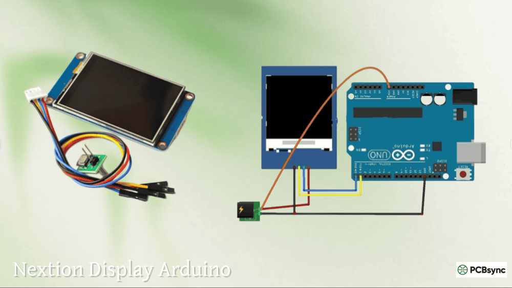
The speed advantage becomes immediately apparent in demanding applications. Updating a 320×240 pixel TFT display requires transferring 153,600 bytes per frame. At I2C’s 400 kHz maximum, this takes over 3 seconds per frame. Using SPI at 8 MHz reduces this to around 150 milliseconds—the difference between an unusable slideshow and smooth animation.
Arduino SPI Pin Configuration
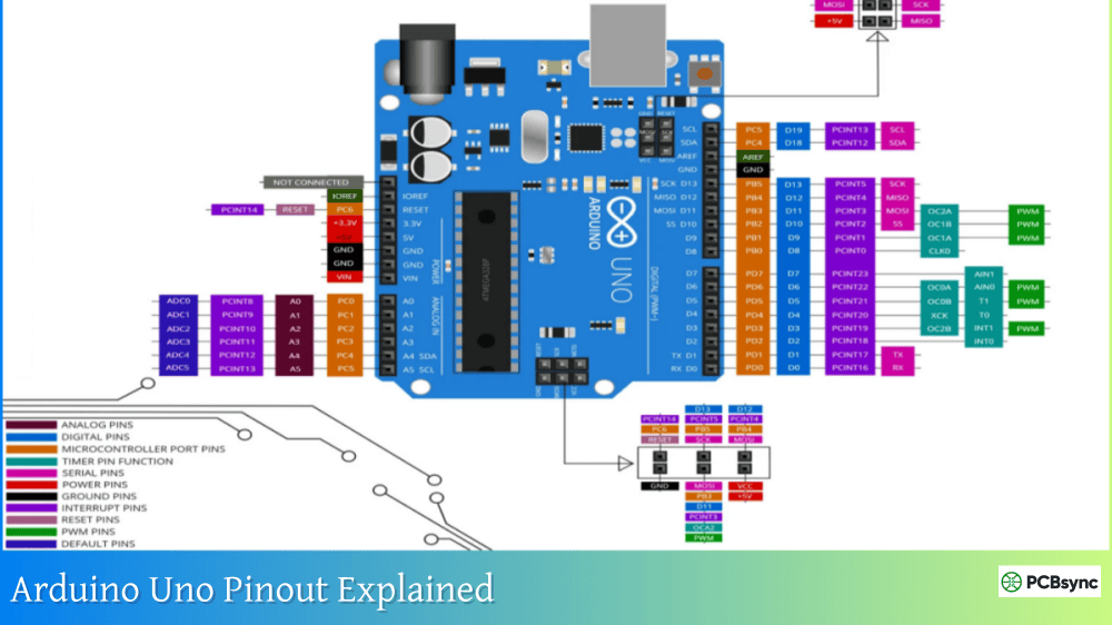
Arduino boards dedicate specific pins to SPI communication, though their physical location varies by board type. These pins connect to the ATmega’s hardware SPI peripheral, providing far superior performance compared to software-based SPI implementations.
Pin Assignments Across Arduino Boards
Board
MOSI
MISO
SCK
SS
ICSP Header
Arduino Uno
Pin 11
Pin 12
Pin 13
Pin 10
Yes
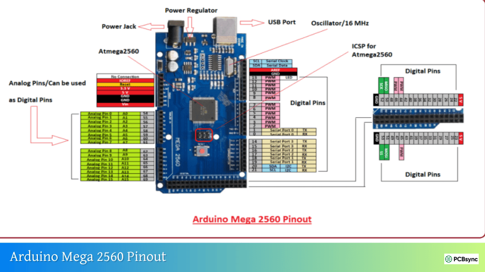
Arduino Mega
Pin 51
Pin 50
Pin 52
Pin 53
Yes
Arduino Leonardo
ICSP-4
ICSP-1
ICSP-3
Pin 10
Yes
Arduino Nano
Pin 11
Pin 12
Pin 13
Pin 10
Yes
Arduino Due
ICSP-4
ICSP-1
ICSP-3
Pin 10
Yes
MOSI (Master Out Slave In): Data line from master to slave. The Arduino outputs data on this pin that slaves read.
MISO (Master In Slave Out): Data line from slave to master. Slave devices output data here that Arduino reads.
SCK (Serial Clock): Clock signal generated by the master. This synchronizes all data transmission—every bit transfer occurs on a clock edge.
SS (Slave Select): Also called CS (Chip Select). The master pulls this line LOW to select which slave device should respond to commands. Each slave requires its own unique SS pin.
The ICSP (In-Circuit Serial Programming) header provides an alternative access point to SPI pins, particularly useful on boards where the digital pins are occupied. However, MOSI, MISO, and SCK on the ICSP header are electrically identical to the corresponding digital pins—using ICSP doesn’t free up the digital pins for other purposes.
SPI Clock Modes: CPOL and CPHA Explained
The relationship between clock and data presents timing challenges that SPI addresses through four distinct modes, defined by two parameters: Clock Polarity (CPOL) and Clock Phase (CPHA). Both master and slave must use identical mode settings for successful communication—mismatched modes result in corrupted data or complete communication failure.
Clock Polarity (CPOL)
CPOL determines the idle state of the clock signal—the voltage level when no data is being transmitted:
CPOL = 0: Clock idles LOW. The first clock edge is rising (LOW to HIGH).
CPOL = 1: Clock idles HIGH. The first clock edge is falling (HIGH to LOW).
Clock Phase (CPHA)
CPHA determines whether data is sampled on the leading or trailing clock edge:
CPHA = 0: Data is sampled on the leading edge, shifted on the trailing edge.
CPHA = 1: Data is sampled on the trailing edge, shifted on the leading edge.
The Four SPI Modes
Mode
CPOL
CPHA
Clock Idle State
Sample Edge
Shift Edge
Typical Devices
0
0
0
LOW
Rising
Falling
Most common—SD cards, many sensors
1
0
1
LOW
Falling
Rising
Some ADCs and DACs
2
1
0
HIGH
Falling
Rising
Less common
3
1
1
HIGH
Rising
Falling
Some displays and EEPROMs
Mode 0 dominates real-world applications—if device documentation doesn’t specify the required mode, try Mode 0 first. The critical detail: check your peripheral’s datasheet for timing diagrams showing clock polarity and data sampling edges. Guessing the wrong mode wastes hours debugging phantom communication errors.
Programming Arduino SPI: Essential Functions
The Arduino SPI library abstracts the complexity of register manipulation, providing clean high-level functions for SPI communication. Include the library with #include <SPI.h> at the beginning of your sketch.
Core SPI Library Functions
SPI.begin(): Initializes the SPI bus, configuring MOSI, MISO, and SCK pins as appropriate and setting them to their idle states.
void setup() {
SPI.begin();
}
SPI.beginTransaction(settings): Configures SPI parameters for a specific device. This function should precede every communication sequence.
Clock speed (Hz): Maximum frequency for this device (e.g., 4000000 for 4 MHz)
Bit order: MSBFIRST (most significant bit first) or LSBFIRST
Data mode: SPI_MODE0, SPI_MODE1, SPI_MODE2, or SPI_MODE3
SPI.transfer(data): Sends a byte while simultaneously receiving a byte. SPI’s full-duplex nature means transmission and reception occur concurrently—the returned byte comes from the slave.
byte received = SPI.transfer(0xAA);
SPI.endTransaction(): Releases the SPI bus, allowing other devices (if any) to use it.
SPI.end(): Disables the SPI bus, returning pins to general I/O mode.
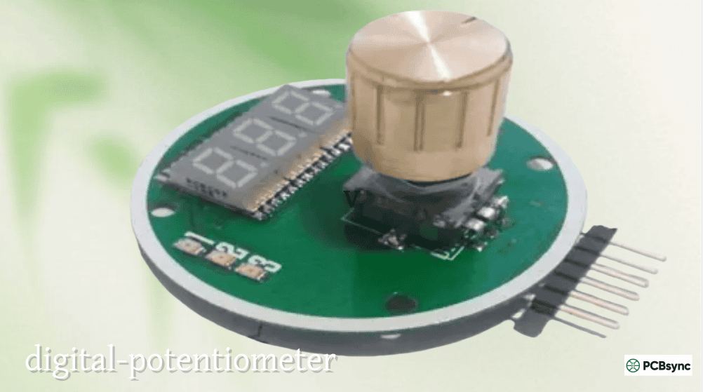
Complete Arduino SPI Example: Communicating with Digital Potentiometer
Let’s implement a practical example controlling an MCP4131 digital potentiometer via SPI. This 7-bit device (129 positions) provides 0-10kΩ resistance adjustment through simple SPI commands.
Wiring MCP4131 to Arduino Uno
MCP4131 Pin 1 (CS) → Arduino Pin 10
MCP4131 Pin 2 (SCK) → Arduino Pin 13
MCP4131 Pin 3 (SI) → Arduino Pin 11
MCP4131 Pin 4 (VSS) → GND
MCP4131 Pin 5 (PA0) → Multimeter positive probe
MCP4131 Pin 6 (PW0) → Multimeter negative probe
MCP4131 Pin 7 (PB0) → GND
MCP4131 Pin 8 (VDD) → 5V
MCP4131 Control Code
#include <SPI.h>
const int CS_PIN = 10;
void setup() {
Serial.begin(115200);
pinMode(CS_PIN, OUTPUT);
digitalWrite(CS_PIN, HIGH); // Deselect initially
SPI.begin();
SPI.setClockDivider(SPI_CLOCK_DIV4); // 4 MHz on 16 MHz Arduino
Serial.println(“MCP4131 Digital Potentiometer Control”);
}
void loop() {
for (int position = 0; position < 129; position++) {
setPotentiometer(position);
Serial.print(“Wiper position: “);
Serial.println(position);
delay(50);
}
delay(1000);
}
void setPotentiometer(byte position) {
// MCP4131 command: write to wiper register (address 0x00)
byte data = position & 0x7F; // 7-bit position (0-128)
digitalWrite(CS_PIN, LOW); // Select device
SPI.transfer(command);
SPI.transfer(data);
digitalWrite(CS_PIN, HIGH); // Deselect device
}
This code sweeps through all 129 potentiometer positions, demonstrating the basic SPI transaction pattern: assert CS, transfer data bytes, deassert CS. Monitor resistance between PA0 and PW0 with a multimeter to verify operation.
Managing Multiple SPI Slave Devices
Real projects often require multiple SPI peripherals—an SD card for data logging, a display for visualization, and an ADC for high-precision measurements. Each device needs its own slave select (SS/CS) pin, while MOSI, MISO, and SCK connect in parallel across all devices.
Multi-Device Wiring Strategy
Arduino Pin 11 (MOSI) → All slave devices’ MOSI/DI pins
Arduino Pin 12 (MISO) → All slave devices’ MISO/DO pins
Arduino Pin 13 (SCK) → All slave devices’ SCK pins
Arduino Pin 10 (CS1) → Device 1 CS pin
Arduino Pin 9 (CS2) → Device 2 CS pin
Arduino Pin 8 (CS3) → Device 3 CS pin
Critical rule: Only one CS pin should be LOW at any time. Multiple simultaneously selected slaves corrupt data as they all attempt driving the MISO line together. Before selecting a new device, ensure the previous device’s CS returns HIGH.
The beginTransaction() and endTransaction() functions allow different SPI settings for each device, automatically configuring clock speed and mode when switching between peripherals. This proves essential when devices have conflicting requirements—perhaps your ADC requires 2 MHz with Mode 1 while your display wants 10 MHz with Mode 0.
Common Arduino SPI Pitfalls and Solutions
Problem: Garbled Data or No Communication
Symptoms: SPI.transfer() returns unexpected values, device doesn’t respond to commands.
Solutions: Verify clock mode matches device requirements—Mode 0 works for most devices but check datasheets. Confirm clock speed doesn’t exceed device maximum—many sensors limit to 1-4 MHz even though Arduino supports 8+ MHz. Check wiring especially MISO/MOSI reversal (easy mistake causing bidirectional failure). Ensure CS idles HIGH and only goes LOW during active transactions. Verify common ground between Arduino and all SPI devices—floating grounds cause erratic behavior.
Problem: Intermittent Communication Failures
Symptoms: Communication works sometimes but randomly fails or corrupts data.
Solutions: Reduce clock speed—long wires act as transmission lines with impedance and capacitance that distort high-frequency signals. Keep SPI wiring under 6 inches when possible. Add 10-100pF capacitors between SCK and ground near each slave device to filter clock edges. Use separate bypass capacitors (0.1µF) on each device’s power pins placed close to the chip. Verify multiple slaves don’t have CS asserted simultaneously—add debugging Serial.print() statements showing CS state changes.
Problem: Slow Data Transfer Despite High Clock Speed
Symptoms: Large transfers take longer than expected based on clock frequency.
Solutions: Use SPI.transfer() in loops rather than individual transactions for bulk data. The transaction overhead (beginTransaction, CS manipulation, endTransaction) adds microseconds per byte—acceptable for occasional commands but devastating for kilobyte transfers. For Arduino Mega, use hardware CS control via SPDR register for fastest possible transfers. Ensure interrupts aren’t disrupting timing—disable with noInterrupts() during critical SPI sequences, re-enable with interrupts() afterward.
No installation required—included with Arduino IDE
Examples: File → Examples → SPI
SPIMemory Library: Specialized library for SPI Flash and EEPROM chips
GitHub: https://github.com/Marzogh/SPIMemory
Simplifies reading/writing common memory chips
Includes wear-leveling and power-loss protection
SD Library: Standard library for SD card communication via SPI
Included with Arduino IDE
Handles FAT filesystem and file operations
Works with standard SD and microSD cards
Hardware Datasheets and Specifications
Resource
Description
Application
MCP4131 Datasheet
Digital potentiometer specifications
Learning basic SPI control
25LC1024 Datasheet
1Mbit SPI EEPROM
Non-volatile storage projects
ILI9341 Datasheet
TFT display controller
Graphics applications
MCP3008 Datasheet
8-channel 10-bit ADC
Analog sensing via SPI
nRF24L01+ Datasheet
2.4GHz wireless transceiver
Wireless SPI communication
Testing and Debugging Tools
Logic Analyzer: Capture and decode SPI transactions showing exact timing, data values, and protocol violations. Budget analyzers like DSLogic or Saleae Logic work excellently for SPI debugging at speeds up to several MHz.
Oscilloscope: View actual waveforms on SCK, MOSI, and MISO to diagnose signal integrity issues—ringing, overshoot, or inadequate voltage levels all visible on scope traces.
Multimeter: Verify supply voltage at each device, confirm common ground between all nodes, and check CS pin states to ensure proper device selection.
Advanced Arduino SPI Techniques
Optimizing Transfer Speed with Direct Register Access
While the SPI library provides convenience, direct register manipulation achieves maximum performance for time-critical applications. The SPDR (SPI Data Register) directly controls the hardware SPI peripheral.
// Fastest possible 8-byte transfer (no error checking)
void fastSPITransfer(byte *data, int length) {
for (int i = 0; i < length; i++) {
SPDR = data[i]; // Load byte into SPI data register
while (!(SPSR & (1 << SPIF))); // Wait for transfer complete
data[i] = SPDR; // Read received byte
}
}
This method eliminates function call overhead and library abstraction layers, shaving precious microseconds from each byte transfer. Critical for maintaining frame rates in display updates or meeting timing requirements in motor control applications.
Implementing DMA for Zero-CPU SPI Transfers
Arduino Due’s SAM3X processor supports DMA (Direct Memory Access) for SPI, allowing transfers without CPU intervention. While complex to configure, DMA enables the processor to perform calculations while simultaneously streaming kilobytes to displays or memory.
The technique involves configuring DMA channels to automatically feed SPI peripheral from memory buffers, interrupt-driven to signal completion. Particularly valuable for audio streaming, real-time sensor data logging, or any application where CPU cycles are precious.
Frequently Asked Questions
Q: Can I use any digital pin as the SPI slave select (SS/CS) pin?
A: Yes, any digital output pin can serve as SS/CS for slave devices. The Arduino SPI library doesn’t strictly require using pin 10 as SS—that’s merely convention. However, pin 10 has special significance: if configured as INPUT, the Arduino can act as an SPI slave rather than master. For master mode operation, either set pin 10 as OUTPUT (even if not used for any device) or physically connect it HIGH to prevent accidental slave mode. Most developers configure pin 10 as OUTPUT and use it as the first device’s CS pin to avoid this potential pitfall.
Q: Why does my Arduino SPI communication work on breadboard but fail on PCB?
A: Breadboards introduce capacitance (typically 2-5pF per connection point) and inductance from long tie strips, plus resistance from oxidized spring contacts. These parasitics limit practical SPI speeds to 1-2 MHz on breadboards. PCBs with proper ground planes, controlled impedance traces, and minimal trace length support 10+ MHz reliably. The solution: test at lower speeds during breadboarding (1 MHz or less), then increase speed after transitioning to PCB. Also verify your PCB includes proper bypass capacitioning—0.1µF ceramic capacitor within 10mm of each IC’s VCC pin. Flying wire connections or poor ground planes cause voltage droops during SPI transactions that breadboards’ solid ground buses don’t exhibit.
Q: Can I connect 3.3V SPI devices to 5V Arduino boards safely?
A: Not directly—5V logic levels from Arduino outputs will damage 3.3V device inputs over time, and 3.3V device outputs may not reliably register as logic HIGH on 5V Arduino inputs (threshold typically 2.5V). Use bidirectional level shifters (like TXS0108E) or voltage dividers (10kΩ and 20kΩ resistors for 5V→3.3V direction) on all signal lines: MOSI, SCK, and CS. MISO from 3.3V device to 5V Arduino typically works without level shifting since 3.3V exceeds the 2.5V threshold, though proper level shifters provide better noise margins. Alternatively, use 3.3V Arduino boards (Due, Zero, MKR series) which natively operate at 3.3V logic levels.
Q: What’s the maximum SPI clock speed I can use with Arduino?
A: Hardware limitations and practical considerations both constrain maximum SPI speeds. Arduino Uno and Nano (16 MHz system clock) support SPI speeds up to 8 MHz (system clock divided by 2). Arduino Mega same specifications. Arduino Due (84 MHz system clock) theoretically supports up to 42 MHz but practical limits around 20-25 MHz due to poor signal integrity at extreme speeds. However, wiring quality typically becomes the bottleneck before reaching hardware limits—breadboards fail above 2 MHz, PCB traces longer than 3 inches limit to 4-6 MHz, proper impedance-controlled routing enables 10+ MHz. Additionally, slave devices impose their own maximum clock frequencies (SD cards typically limit to 25-50 MHz, older sensors to 1-4 MHz). Always consult device datasheets and test thoroughly at target speeds.
Q: How do I debug SPI communication when nothing works?
A: Systematic troubleshooting isolates issues quickly. First, verify physical connections with multimeter continuity testing—check each wire individually. Second, confirm voltage levels: measure 5V (or 3.3V) at each device’s VCC pin under load, verify CS pin voltage transitions HIGH/LOW when toggled. Third, use simplest possible test: control a digital potentiometer or flash LED via SPI commands—if this works, your SPI hardware functions correctly and problems lie in device-specific protocols. Fourth, reduce clock speed to absolute minimum (62.5 kHz on Uno) to eliminate signal integrity issues. Fifth, add Serial.print() debugging showing exact bytes transmitted/received and CS pin states. Finally, if available, use logic analyzer to capture complete transactions—seeing actual waveforms and decoded bytes reveals timing violations, incorrect modes, or protocol errors invisible to code-based debugging.
Conclusion
Arduino SPI communication provides the high-speed, full-duplex interface essential for demanding embedded applications. Mastering SPI opens doors to rapid data acquisition through ADCs, vivid graphics on TFT displays, reliable data logging to SD cards, and countless peripherals that communicate faster than I2C or UART allow.
The protocol’s simplicity—just four wires and straightforward transaction sequences—belies the nuanced understanding required for reliable operation. Clock mode selection, proper CS timing, signal integrity at high speeds, and multi-device coordination all demand attention to detail that separates working prototypes from production-quality designs.
Whether you’re building sensor data loggers capturing measurements at kilohertz rates, developing graphical user interfaces requiring rapid screen updates, or designing communication systems demanding maximum throughput, the techniques and knowledge presented here establish the foundation for successful SPI implementations. Start with simple single-device projects, experiment with different clock speeds and modes, then scale to complex multi-peripheral systems with confidence.
Inquire: Call 0086-755-23203480, or reach out via the form below/your sales contact to discuss our design, manufacturing, and assembly capabilities.
Quote: Email your PCB files to Sales@pcbsync.com (Preferred for large files) or submit online. We will contact you promptly. Please ensure your email is correct.
Notes: For PCB fabrication, we require PCB design file in Gerber RS-274X format (most preferred), *.PCB/DDB (Protel, inform your program version) format or *.BRD (Eagle) format. For PCB assembly, we require PCB design file in above mentioned format, drilling file and BOM. Click to download BOM template To avoid file missing, please include all files into one folder and compress it into .zip or .rar format.


