Inquire: Call 0086-755-23203480, or reach out via the form below/your sales contact to discuss our design, manufacturing, and assembly capabilities.
Quote: Email your PCB files to Sales@pcbsync.com (Preferred for large files) or submit online. We will contact you promptly. Please ensure your email is correct.
Notes: For PCB fabrication, we require PCB design file in Gerber RS-274X format (most preferred), *.PCB/DDB (Protel, inform your program version) format or *.BRD (Eagle) format. For PCB assembly, we require PCB design file in above mentioned format, drilling file and BOM. Click to download BOM template To avoid file missing, please include all files into one folder and compress it into .zip or .rar format.
After spending over a decade on assembly lines watching millions of components get placed, I can tell you that surface mount technology has fundamentally changed how we build electronics. Let me walk you through what makes this process so crucial for modern manufacturing.
Understanding Surface Mount PCB Assembly
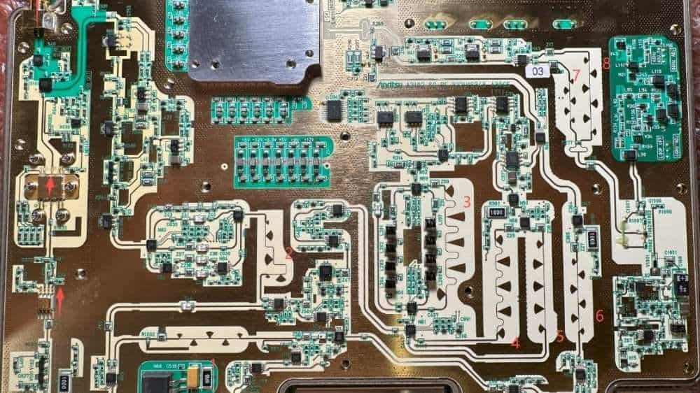
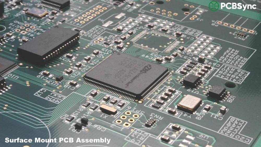
Surface Mount PCB Assembly is a manufacturing method where electronic components mount directly onto the PCB surface rather than inserting through drilled holes. Think of it like building with LEGO blocks that stick flat on a board versus pushing pegs through holes. The components, called Surface Mount Devices (SMDs), attach to copper pads using solder paste and reflow soldering.
I remember when IBM first developed this approach back in the 1960s for small-scale computers. By the 1980s, it became mainstream, and today it accounts for roughly 80-85% of all PCB assembly work. The shift happened because manufacturers needed smaller, faster, and cheaper electronics to meet consumer demands.
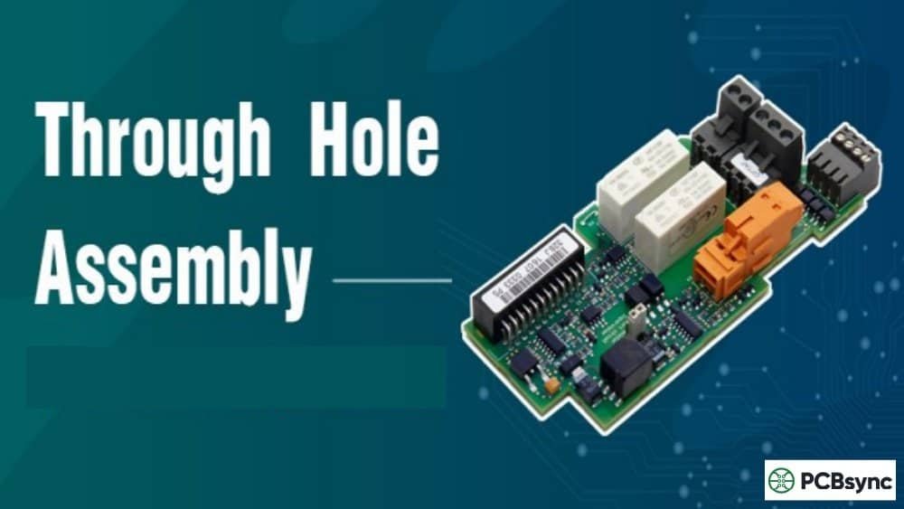
The key difference from traditionalthrough-hole technology is simple: no drilling required. Components sit on the surface, leads are shorter (or nonexistent), and everything happens much faster. A modern SMT line can place over 136,000 components per hour, compared to maybe a few thousand with through-hole assembly.
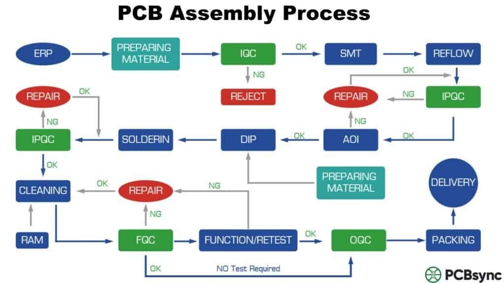
Walking through an actual assembly line reveals exactly how boards transform from bare copper to finished products. Each step requires precision, but the automation makes it repeatable and reliable.
Step 1: Solder Paste Printing
The process starts with applying solder paste to the bare PCB. We use a stainless steel stencil with laser-cut apertures that align perfectly with the pad locations. The stencil sits on top of the PCB, and a squeegee pushes solder paste through the openings.
The paste itself is a mixture of tiny solder balls suspended in flux. Getting the right amount is critical – too much creates bridges between pads, too little results in weak joints. Modern printers include 3D inspection systems that check paste height and volume immediately after printing.
Temperature matters here. I always recommend keeping the paste between 20-25°C and using it within 24 hours after opening. Some advanced facilities use nitrogen jet printing for ultra-fine pitch components, but stencil printing handles 95% of applications.
Step 2: Solder Paste Inspection (SPI)
Before placing any components, we verify the paste application. Automated SPI systems use lasers and cameras to measure paste volume, height, and position in 3D. The machine compares measurements against programmed tolerances, typically ±25% for volume and ±50 microns for position.
Catching defects here saves enormous costs. Fixing a paste issue costs maybe $0.50 per board. Missing it means rework after reflow, which can cost $15-30 per board. That’s why experienced manufacturers won’t skip this step, even for prototypes.
Step 3: Component Placement
This is where the magic happens. Pick-and-place machines use vacuum nozzles to grab components from tape reels or trays and position them on the solder paste. The machines work from CAD data (Gerber files and pick-and-place files) to know exactly where each component goes.
Modern placement machines have vision systems that check component orientation and alignment in real-time. If a part is misaligned by more than half a pad width, the machine rejects it. High-speed machines can place 80,000-100,000 components per hour, while high-accuracy machines sacrifice some speed for ultra-fine pitch components like 01005 resistors or 0.4mm pitch BGAs.
The placement sequence matters. We typically place smaller passive components first, then ICs, and finally connectors or larger parts. This prevents shadows that could interfere with vision systems.
Step 4: Pre-Reflow Inspection
Before sending boards into the oven, a quick visual check catches obvious issues. Some facilities use automated optical inspection (AOI) here, but many rely on trained operators who can spot problems in seconds. They look for missing components, tombstoning (where one end of a component lifts up), or parts that shifted during placement.
For prototype runs or first articles, this inspection is mandatory. For high-volume production, the pre-reflow check might be statistical sampling rather than 100% inspection.
Step 5: Reflow Soldering
The reflow oven is where components actually solder to the board. Boards travel through multiple temperature zones on a conveyor belt. A typical SAC305 lead-free profile includes:
Activate flux, ensure even temperature across board
Reflow
230-250°C
30-60 seconds
Melt solder, create metallurgical bonds
Cooling
200°C to ambient
60-90 seconds
Solidify solder joints without thermal stress
Peak temperature hits around 235-245°C for lead-free solder, about 20-30°C above the solder’s melting point. The entire cycle takes 4-8 minutes depending on board complexity and thermal mass.
One thing I learned the hard way: temperature profiling is not optional. Different boards need different profiles based on their mass, component types, and layer count. We use thermocouples attached to test boards to validate profiles before production.
Step 6: Post-Reflow Inspection
After reflow, automated optical inspection (AOI) systems check every solder joint. Modern 3D AOI uses multiple cameras and structured light to measure joint height, fillet shape, and volume. The system flags defects like:
Solder bridges (shorts between adjacent pads)
Insufficient solder (weak joints)
Missing components
Tombstoning or billboarding
Solder balls
Component misalignment
For critical applications like medical devices or aerospace, we add X-ray inspection to check hidden joints under BGAs and QFNs. X-ray reveals voids in solder joints that AOI cannot see.
Step 7: Cleaning (Optional)
If you used no-clean flux, this step skips. But for water-soluble or rosin flux, cleaning removes residues that could cause corrosion or leakage currents. The cleaning process uses either aqueous (water-based) or solvent cleaners in batch or inline systems.
Military and medical applications typically require cleaning regardless of flux type. Consumer electronics often skip it to save costs and time.
Step 8: Functional Testing
The final step verifies that the assembled board actually works. This might include:
Can place components on both sides, higher density
Limited by hole spacing, lower density
Assembly Speed
80,000+ components/hour
1,000-2,000 components/hour
Production Cost
Lower for high volume ($0.0015-0.002/joint)
Higher due to manual labor
Mechanical Strength
Moderate, relies on solder joint
Excellent, leads pass through board
Thermal Resistance
Good for most applications
Better for high-power components
Prototype Ease
Requires specialized equipment
Easier for hand assembly
Vibration Resistance
Adequate for most uses
Superior for harsh environments
Signal Performance
Better high-frequency performance
Higher parasitic inductance/capacitance
Drilling Required
Minimal (only vias)
Every component needs holes
Setup Cost
Higher initial investment
Lower for small runs
Best Applications
Consumer electronics, mobile devices, computers
Military, aerospace, power supplies, connectors
The reality is that most modern boards use both. We call this “mixed technology” assembly. You’ll see SMT for the logic and passive components, with through-hole for power connectors, test points, or components that need mechanical stability.
Major Benefits of Surface Mount Assembly
Let me break down why SMT dominates modern electronics from an engineering standpoint:
1. Miniaturization and Space Efficiency
Components are roughly 60-80% smaller than through-hole equivalents. A 0603 resistor (1.6mm x 0.8mm) does the same job as a through-hole resistor that’s 10mm long. You can pack components on both sides of the board, effectively doubling your usable real estate.
I’ve seen boards go from 100mm x 100mm with through-hole to 50mm x 50mm with SMT, using the same circuit design. That size reduction cascades through the entire product, allowing smaller enclosures, lower shipping costs, and better consumer appeal.
2. Manufacturing Speed and Automation
The automation level in SMT is remarkable. A fully automated line with minimal operators can produce thousands of boards daily. Placement speed of 80,000-136,000 components per hour versus 1,000-2,000 for through-hole means dramatically shorter production cycles.
When we switched a product line from through-hole to SMT, assembly time dropped from 2 hours per board to 12 minutes. That’s a 10x improvement in throughput.
3. Cost Reduction
While setup costs are higher (stencils, programming, tooling), the per-unit cost drops significantly at scale. Fewer drilling operations, less material waste, lower labor costs, and faster production all contribute to savings.
For production runs over 100 units, SMT typically costs 30-50% less than through-hole. The crossover point depends on complexity, but generally happens around 50-100 boards.
4. Electrical Performance
Shorter lead lengths mean lower parasitic inductance and capacitance. This dramatically improves high-frequency performance. I’ve measured 40-60% reduction in parasitic effects compared to through-hole components, which translates to better signal integrity above 100 MHz.
The lower resistance also reduces power loss and heat generation in power circuits.
5. Reliability and Consistency
Automated processes reduce human error. When a through-hole board requires 500 manual solder joints, the defect rate might be 0.1-0.5%. With SMT automation, we regularly achieve defect rates below 50 PPM (parts per million), sometimes down to 10 PPM with proper process control.
The solder joints themselves, when properly formed, are actually quite robust. Surface tension during reflow provides self-alignment, helping correct minor placement errors.
6. Design Flexibility
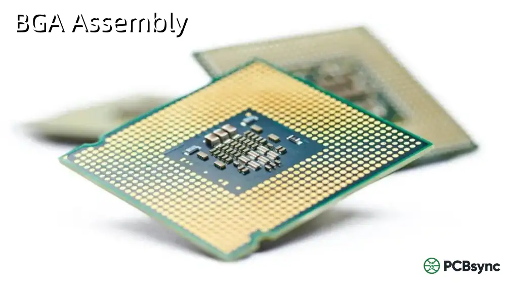
SMT components come in package varieties that through-hole cannot match. Ball Grid Arrays (BGAs), Quad Flat No-leads (QFNs), and chip-scale packages allow integration levels impossible with through-hole technology.
Modern microcontrollers with 200+ I/O pins would be impractical in through-hole packages but work perfectly in fine-pitch QFP or BGA formats.
Cost Factors in SMT Assembly
Understanding what drives cost helps you budget accurately and optimize designs for manufacturability. Let me break down the major cost components based on actual manufacturing data.
These costs are amortized across the production run. For 10 boards, setup might add $50 per board. For 1,000 boards, it’s $0.50 per board.
Per-Unit Assembly Costs
The main variables include:
1. Component Placement Typical pricing ranges from $0.0015 to $0.003 per solder joint. A board with 200 SMT components averaging 4 pads each (800 joints) costs $1.20-2.40 just for placement.
2. Component Sourcing This is often the largest cost. Components range from pennies for basic resistors to hundreds of dollars for complex ICs. Turnkey assembly (where the CM buys components) includes markup of 10-25%. Consignment (you provide components) eliminates markup but transfers procurement risk to you.
3. Board Complexity Simple single-sided boards cost less than complex double-sided boards with fine-pitch components. BGA and micro-BGA packages require X-ray inspection, adding cost. Very fine pitch (0.4mm or less) may require high-precision placement equipment, potentially doubling placement costs.
4. Production Quantity
Quantity
Estimated Cost Per Board*
Key Driver
1-10 (Prototype)
$150-500+
Setup costs dominate
25-100
$75-200
Moderate economies of scale
100-500
$40-100
Better component pricing
500-1,000
$25-60
Volume discounts kick in
1,000-10,000
$15-40
Optimized production flow
10,000+
$8-25
Maximum efficiency
*Assumes moderate complexity, includes components, PCB, and assembly
5. Testing Requirements Basic visual inspection costs minimal. AOI adds $0.50-2.00 per board. Flying probe testing costs $3-8 per board. ICT with fixture costs $0.50-2.00 per board (after fixture amortization). Functional testing varies widely based on complexity, from $2-20+ per board.
6. Lead Time Standard lead time (5-10 business days) uses standard pricing. Expedited service (24-72 hours) typically adds 50-200% premium. Rush orders disrupt production schedules and require overtime, justifying the premium.
Cost Optimization Strategies
From years of manufacturing experience, here are practical ways to reduce costs:
Aerospace and Defense: Avionics, radar systems, communication equipment, guidance systems, satellites (note: often combined with through-hole for critical connections)
Key Challenges and Solutions in SMT Manufacturing
No process is perfect. Here are the real challenges I’ve encountered and how we solve them:
Challenge 1: Component Tombstoning Small passive components sometimes stand up on one end during reflow. This happens due to uneven heating or paste distribution.
Solution: Symmetrical pad design, proper thermal profiling, adequate paste volume, and slower ramp rates during preheat.
Challenge 2: Solder Bridging Excess solder creates shorts between adjacent pads, especially on fine-pitch ICs.
Solution: Optimize stencil thickness and aperture design (often use reduced apertures for fine pitch), maintain paste viscosity, ensure proper squeegee pressure.
Challenge 3: Void Formation in BGAs Trapped gas or flux residues create voids in solder balls, weakening joints.
Solution: Proper reflow profile with adequate soaking time, use of vacuum reflow for critical applications, nitrogen atmosphere to reduce oxidation.
Challenge 4: Component Shift Parts move during transport to reflow oven or early in the heating cycle.
YouTube channels focused on PCB assembly (e.g., EEVblog, Strange Parts)
Process Optimization Tools:
KIC thermal profilers (industry standard for reflow profiling)
SPC (Statistical Process Control) software for quality monitoring
AOI programming software from equipment vendors
Pick-and-place optimization software
Frequently Asked Questions (FAQs)
Q1: What is the minimum order quantity for SMT assembly?
Most contract manufacturers will handle prototype quantities starting from a single board, though costs per unit will be highest. The economic sweet spot for professional CM services typically starts around 25-100 boards. Some online services like JLCPCB or PCBWay specialize in small batches starting from 5 boards at competitive pricing.
For truly tiny quantities (1-5 boards), consider finding a local CM that does NPI (New Product Introduction) work, or use a rapid prototyping service. Expect to pay $200-500 per board for complex assemblies at this scale.
Q2: How long does SMT assembly typically take?
Standard lead time is 5-10 business days after receiving bare PCBs and all components. This includes setup, assembly, inspection, and testing. Prototypes with expedited service can complete in 24-72 hours at premium pricing (typically 50-200% cost increase).
Complex boards requiring extensive testing or boards with specialized components may need 10-15 business days. The actual assembly time is short (minutes to hours), but queue time, component procurement, and testing drive the total duration.
Q3: Can SMT and through-hole components be used on the same board?
Absolutely, and this is extremely common. We call this “mixed technology” assembly. Typically, SMT components are placed and reflowed first. Then through-hole components are inserted and wave soldered or hand soldered.
Common through-hole components on otherwise SMT boards include power connectors, large electrolytic capacitors, transformers, terminal blocks, and test points. These components either need the mechanical strength of through-hole mounting or aren’t available in SMT packages.
Q4: What file formats do I need to provide for SMT assembly?
You’re doing high-volume production (1,000+ units)
Cost is the primary driver
You have a simple, well-documented design
Lead time of 2-4 weeks is acceptable
You’re comfortable managing international shipping and customs
Many companies use a hybrid approach: domestic for prototypes and NPI, offshore for high-volume production. Consider the total landed cost including shipping, duties, inventory carrying costs, and communication overhead, not just the quoted assembly price.
Conclusion
Surface mount PCB assembly represents the current standard in electronics manufacturing, and for good reason. The combination of miniaturization, cost efficiency, speed, and performance makes it the clear choice for the vast majority of applications.
As someone who’s built thousands of boards from simple prototypes to complex medical devices, I can tell you that understanding the SMT process thoroughly pays dividends. Knowing what happens at each step helps you design better boards, communicate effectively with your CM, and troubleshoot issues when they arise.
The technology continues to evolve. Component sizes keep shrinking (01005 resistors are now common, and 008004 packages exist). Placement machines get faster and more accurate. Inspection systems become more sophisticated. But the fundamental process remains the same: print, place, reflow, inspect, test.
Whether you’re a student learning electronics, an engineer developing your first product, or a seasoned professional optimizing production, investing time to truly understand SMT assembly will serve you well throughout your career.
Inquire: Call 0086-755-23203480, or reach out via the form below/your sales contact to discuss our design, manufacturing, and assembly capabilities.
Quote: Email your PCB files to Sales@pcbsync.com (Preferred for large files) or submit online. We will contact you promptly. Please ensure your email is correct.
Notes: For PCB fabrication, we require PCB design file in Gerber RS-274X format (most preferred), *.PCB/DDB (Protel, inform your program version) format or *.BRD (Eagle) format. For PCB assembly, we require PCB design file in above mentioned format, drilling file and BOM. Click to download BOM template To avoid file missing, please include all files into one folder and compress it into .zip or .rar format.


