Inquire: Call 0086-755-23203480, or reach out via the form below/your sales contact to discuss our design, manufacturing, and assembly capabilities.
Quote: Email your PCB files to Sales@pcbsync.com (Preferred for large files) or submit online. We will contact you promptly. Please ensure your email is correct.
Notes: For PCB fabrication, we require PCB design file in Gerber RS-274X format (most preferred), *.PCB/DDB (Protel, inform your program version) format or *.BRD (Eagle) format. For PCB assembly, we require PCB design file in above mentioned format, drilling file and BOM. Click to download BOM template To avoid file missing, please include all files into one folder and compress it into .zip or .rar format.
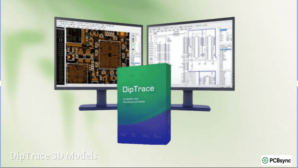
DipTrace PCB Design Tutorial: From Schematic to BOM Export
Learning DipTrace PCB design transformed how I approach circuit board projects. After years working with various EDA tools, I consistently return to DipTrace for its balance of power and accessibility. This tutorial walks you through the complete workflow—from drawing your first schematic to generating a DipTrace BOM ready for component ordering.
Whether you’re exploring the DipTrace PCB design software free download to evaluate it, or you’ve already purchased a license and want to master the workflow, this guide covers everything you need to get a professional PCB manufactured.
Before diving into specifics, let’s establish the complete DipTrace PCB design workflow. Understanding these stages helps you work efficiently and avoid common mistakes.
Stage
DipTrace Module
Output
Schematic Design
Schematic Capture
.dch file
Conversion
Schematic → PCB Layout
Initial .dip file
PCB Layout
PCB Layout
Finalized .dip file
Verification
PCB Layout (DRC/ERC)
Error reports
Output Generation
PCB Layout
Gerber, BOM, Pick & Place
The DipTrace file types you’ll work with most frequently are .dch (schematic) and .dip (PCB layout). Both use XML-based formats in recent versions, making them version-controllable and recoverable if corruption occurs.
If you haven’t installed DipTrace yet, here’s what you need to know about the DipTrace PCB design software free download options:
Version
Limitations
Best For
Freeware
300 pins, 2 signal layers, non-commercial
Learning, simple hobby projects
30-Day Trial
Full features, time-limited
Evaluation before purchase
Starter ($75)
300 pins, 2 signal layers
Small commercial projects
Lite ($145)
500 pins, 2 signal layers
Medium projects
Standard ($395)
1000 pins, 4 signal layers
Professional use
Extended ($695)
2000 pins, 6 signal layers
Complex designs
Full ($995)
Unlimited
Enterprise/advanced
The freeware version includes all features—autorouter, 3D preview, Gerber export—making it genuinely useful for learning DipTrace PCB design. Download from diptrace.com/download/download-diptrace/ and install the 64-bit version for best performance.
Part 1: Creating Your Schematic in DipTrace
The schematic is where every DipTrace PCB design project begins. A well-organized schematic makes PCB layout significantly easier.
Setting Up Your Schematic Document
Launch DipTrace and open Schematic Capture from the launcher. Before placing components:
Configure the sheet: Go to File → Titles and Sheet Setup. Select an appropriate template (ANSI A for simple projects, ANSI B or larger for complex ones). Enable Display Titles and Display Sheet to maintain professional documentation.
Set the grid: View → Grid Setup. I typically use 100 mil (2.54 mm) for component placement, matching standard DIP spacing.
Finding and Placing Components
DipTrace includes over 164,000 components in its standard libraries. To find components:
Method 1: Objects Menu Select Objects → Find Component. Enter the component name or value (e.g., “ATmega328” or “10k resistor”). The search returns matching components from all loaded libraries.
Method 2: Library Browser Click the Library icon on the left toolbar. Navigate through categorized libraries to find components visually.
Method 3: SnapEDA Integration For components not in the standard library, use Objects → Search Parts at SnapEDA. This provides access to over 10 million additional components with symbols, footprints, and 3D models—all free.
Before placing any component, verify the Pattern (footprint) is attached. Click the Pattern button in the component dialog to confirm a footprint exists. A schematic symbol without an attached footprint will cause problems during PCB conversion.
Wiring Your Schematic
With components placed, connect them using wires:
Basic wiring: Hover over a pin until the cursor changes, then click and drag to the destination pin. DipTrace auto-routes the wire with right angles.
Net naming: For power rails and signal buses, use net labels instead of drawing every wire. Place → Net Port creates named connections. Components connected to the same net name are electrically connected even without visible wires.
Buses: For address/data buses, use Place → Bus to create grouped signal paths. This significantly cleans up complex schematics.
Running Electrical Rule Check (ERC)
Before converting to PCB, verify your schematic with Verification → Electrical Rule Check. ERC identifies:
Unconnected pins
Multiple outputs driving the same net
Power pins without connections
Short circuits between power and ground
Fix all errors before proceeding. Warnings can often be ignored (such as unconnected input pins on unused gate sections), but understand each warning before dismissing it.
Saving Your Schematic DipTrace File
Save your schematic (Ctrl+S) before conversion. The DipTrace file will have a .dch extension. I recommend also using File → Save As → DipTrace ASCII for backup—this creates a human-readable version you can recover if the binary file corrupts.
Part 2: Converting Schematic to DipTrace PCB Layout
This is where schematic becomes physical board. The conversion process transfers components and connectivity to PCB Layout.
Initial Conversion Process
In Schematic Capture, select File → Convert to PCB (or press Ctrl+B). The conversion dialog offers options:
Option
When to Use
Use Schematic Rules
First conversion, default settings
Load from File
Apply rules from existing PCB project
Default Rules
Reset to DipTrace defaults
Click OK. DipTrace PCB Layout opens with your components clustered outside a default board outline. The rats nest (thin lines) shows required connections.
Arranging Components
The initial placement is chaotic—that’s normal. Organize components using these approaches:
Automatic arrangement: Placement → Arrange Components clusters components near the board center based on connectivity. This provides a starting point but rarely produces optimal results.
Placement by list: Placement → Placement by List opens a table of all components. Click a component to highlight it, then place it precisely. This method excels for organized, systematic placement.
Manual drag-and-drop: Simply drag components to desired locations. Use Spacebar to rotate components 90 degrees. Ctrl+click selects multiple components for group movement.
Drawing the Board Outline
Before routing, define your board shape:
Select the Board Outline tool from the toolbar (or Route → Board Outline). Draw the perimeter of your PCB. For rectangular boards, click four corners and press Enter. For complex shapes, trace the exact outline needed.
DipTrace supports cutouts using the Board Cutout tool for mounting holes or component clearances.
Setting Design Rules
Before routing, configure design rules that match your PCB manufacturer’s capabilities:
These values work for most standard PCB houses. For budget manufacturers, use 10 mil traces and clearances minimum.
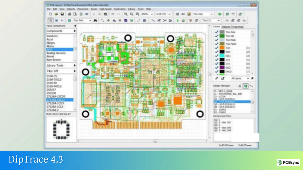
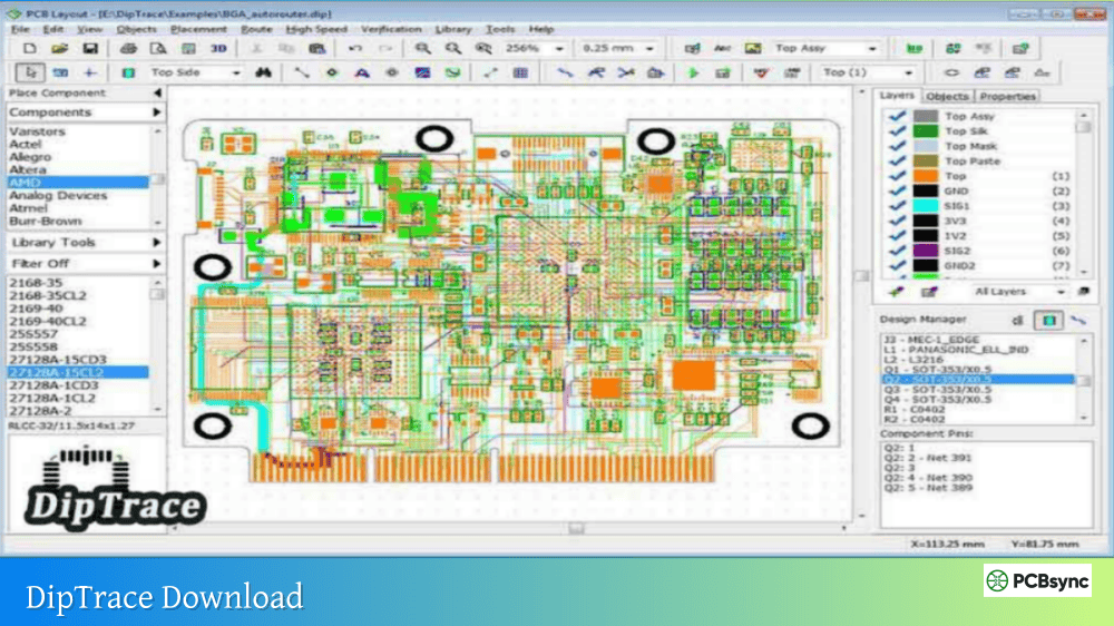
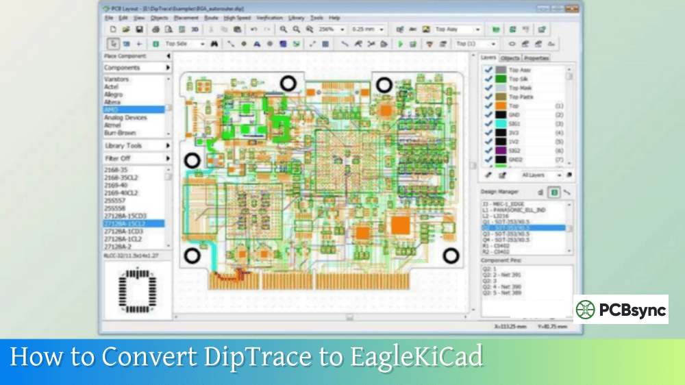
Part 3: Routing Your DipTrace PCB
Routing—connecting components with copper traces—is the core of DipTrace PCB design. DipTrace offers both manual and automatic routing.
Manual Routing Basics
Manual routing provides maximum control. Select Route → Route Manual (or press the routing button on toolbar).
To route a connection:
Click a pad to start
Click intermediate points to set trace path
Click the destination pad to complete
Routing tips from experience:
Route critical signals (clocks, differential pairs) first
Keep power traces wider than signal traces
Use 45-degree angles rather than 90-degree corners
Minimize via count—each via adds resistance and potential reliability issues
Changing layers: Double-click while routing to place a via and switch layers. Or right-click a trace segment and select Segment Layer → Top/Bottom.
Using the Autorouter
DipTrace includes a shape-based autorouter that handles many designs competently:
Go to Route → Route Setup
Configure trace width, clearance, and via parameters
Select Route → Run Autorouter (or press F9)
The autorouter works iteratively. If it can’t complete all connections, it reports unrouted nets. You can then manually route difficult connections and re-run the autorouter for remaining nets.
Autorouter tip: Set layer direction preferences. For two-layer boards, configure top layer for horizontal traces and bottom for vertical (or vice versa). This helps the autorouter achieve cleaner results.
Adding Copper Pours (Ground Planes)
Copper pours fill unused board areas with copper, typically connected to ground. Benefits include reduced EMI, improved thermal dissipation, and lower manufacturing costs (less etching).
To create a copper pour:
Select Route → Place Copper Pour
Draw the pour boundary (cover the entire board for a full ground plane)
Press Enter to complete the shape
In the properties dialog, set Connect to Net: GND
Choose thermal relief style (4-spoke recommended)
Set appropriate clearance values
The pour automatically flows around traces and pads while maintaining clearances.
Part 4: DipTrace Update PCB from Schematics
Real projects require iteration. You’ll modify the schematic after starting PCB layout. The DipTrace update PCB from schematics feature synchronizes changes without losing your layout work.
Understanding Synchronization Methods
DipTrace offers three methods for DipTrace update PCB from schematics:
Method
Use When
How It Works
By Components
Original DipTrace schematic
Uses hidden component IDs
By RefDes
Imported designs or renamed components
Matches by reference designator
By Related Schematic
Quick update, same schematic
Like “By Components” but auto-selects file
Step-by-Step Update Process
In Schematic Capture:
Make your changes (add/remove components, modify connections)
Save the schematic file (Ctrl+S)
In PCB Layout:
Select File → Renew Layout from Schematic
Choose the appropriate method:
“By Related Schematic” for typical updates (Ctrl+Alt+U)
“By RefDes” if you’ve renamed components or imported from another tool
Select the schematic file if prompted
Click OK
New components appear outside the board outline. Deleted components are removed. Modified connections update the rats nest. Existing placement and routing for unchanged components remains intact.
Handling Common Update Issues
“Components moved outside board after update”
This usually means hidden IDs no longer match between schematic and PCB. Solution: Use “By RefDes” update once to re-establish the link, then subsequent updates can use “By Components.”
“Traces disappeared after update”
If a component’s pins changed (different pattern or pin numbering), traces connecting to it are removed. This is actually correct behavior—the old routing may be invalid. Re-route affected connections manually.
Back Annotation: PCB to Schematic
Sometimes you modify the PCB and need to push changes back to the schematic. In Schematic Capture, use File → Back Annotate to synchronize:
Reference designator changes
Component values
Net names
Component types
Back annotation doesn’t add new components or nets—it only updates existing properties.
Part 5: Verification and Design Rule Check
Before generating manufacturing files, thoroughly verify your design.
Clearance violations between traces, pads, and copper
Trace width violations
Via specifications
Differential pair constraints
Silkscreen clearances
DRC runs against the rules you configured in Route → Design Rules. Fix all errors before manufacturing. Most PCB houses run their own DRC and will reject boards with violations.
Net Connectivity Check
Verification → Net Connectivity ensures all nets are properly routed:
Identifies unrouted connections
Finds broken traces
Detects merged nets (shorts)
A clean connectivity check means every connection in your schematic exists on the PCB.
Compare to Schematic
Verification → Compare to Schematic checks that the PCB matches the source schematic:
Components present in both files
Connections match
Reference designators align
This catches issues where PCB and schematic diverged during editing.
3D Preview
Before finalizing, preview your board in 3D: View → 3D Preview. Rotate and zoom to check:
Component heights and clearances
Connector positioning
Mounting hole locations
Overall board appearance
DipTrace includes over 11,000 3D models. Components from SnapEDA typically include 3D models as well.
Can I generate a BOM from PCB Layout instead of Schematic?
No, the DipTrace BOM tool exists only in Schematic Capture. The PCB Layout editor doesn’t include BOM generation. This design decision ensures your BOM matches the design documentation (schematic) rather than the physical implementation. If you need component information from a PCB file without a schematic, export to DipTrace ASCII format and parse the component data programmatically.
Why does “Renew Layout from Schematic” move my components outside the board?
This happens when the hidden component IDs no longer match between schematic and PCB. Common causes include deleting and re-adding components in the schematic, or importing a schematic from another tool. Solution: Use DipTrace update PCB from schematics with the “By RefDes” option once. This re-establishes the ID link. Subsequent updates can use “By Components” or “By Related Schematic” normally.
What’s the difference between DipTrace file formats .dch/.dip and ASCII exports?
The .dch (schematic) and .dip (PCB) files are binary DipTrace file formats optimized for performance. ASCII exports create human-readable text files useful for backup, version control, and troubleshooting. Recent DipTrace versions also support XML format for even better compatibility. For daily work, use the native formats. Export ASCII or XML periodically as backup.
How do I use SnapEDA components that don’t have 3D models?
When placing a SnapEDA component, if a 3D model is available, the “Download 3D Model” button activates. If not, you have options: search the DipTrace 3D library for a compatible generic model, use the built-in IPC-7351 Pattern Generator to create a model automatically, or import a STEP file from the manufacturer’s website. The 3D model attaches in Pattern Editor using Pattern → Attach 3D Model.
Is the DipTrace autorouter good enough for production boards?
The DipTrace shape-based autorouter handles many designs adequately, especially simple to moderate complexity boards. For best results: place components thoughtfully before autorouting, configure proper design rules and layer preferences, and expect to manually clean up 10-20% of the routing afterward. For high-speed designs or dense boards, manual routing typically produces superior results. The autorouter excels at initial routing that you then refine.
Part 8: Advanced DipTrace PCB Techniques
Once you’re comfortable with the basic workflow, these advanced techniques will improve your DipTrace PCB design quality and efficiency.
Working with Multi-Sheet Schematics
Complex projects benefit from organizing circuits across multiple schematic sheets. In Schematic Capture:
Adding sheets: Select Edit → Add Sheet. Each sheet becomes a separate page in your schematic document.
Connecting between sheets: Use hierarchical net ports. Place → Net Port creates a named connection point. Ports with identical names on different sheets are electrically connected. This keeps your main schematic clean while detail pages contain supporting circuits.
Sheet navigation: Use the sheet tabs at the bottom of the Schematic window or View → Sheet Manager for an overview.
Hierarchical Design for Reusable Blocks
For designs with repeated circuit blocks (multiple identical channels, for example), hierarchical design saves time:
Create the repeated circuit as a separate schematic file
In your main schematic, use Place → Hierarchical Block
Point to the sub-schematic file
Place multiple instances of the block
When you convert to PCB, each instance becomes a separate set of components with unique reference designators. Modify the sub-schematic once, and all instances update.
Differential Pair Routing
Modern high-speed designs require differential pair routing for signals like USB, HDMI, and Ethernet. DipTrace handles differential pairs natively:
Defining pairs: In Schematic Capture, right-click a net and select Properties. In the Net Class settings, enable differential pair mode and specify the paired net.
Routing pairs: In PCB Layout, Route → Differential Pair activates paired routing mode. Both traces route simultaneously, maintaining consistent spacing and length matching.
Phase tuning: If your differential pair requires precise length matching, use the Phase Tune tool to add serpentine meanders that equalize trace lengths.
Length Matching for High-Speed Buses
Memory interfaces and other parallel buses require matched trace lengths. DipTrace provides length matching tools:
Define a net class for the matched signals
Set length constraints in the net class properties
Use Route → Length Matching to visualize current lengths
Apply serpentine tuning to shorter traces
The real-time length comparison table shows actual vs. target lengths as you route, making it easy to achieve tight tolerances.
Creating Custom Components
When the standard libraries and SnapEDA don’t have your component, create custom parts:
In Component Editor:
Launch Component Editor from the DipTrace Launcher
Select Component → Add New
Choose a template (DIP, QFP, etc.) or start blank
Define pins using the pin tools
Set electrical properties (input, output, power, etc.)
Attach a pattern (footprint)
In Pattern Editor:
Launch Pattern Editor
Create a new pattern with appropriate pad layout
Use the IPC-7351 Pattern Generator for standard packages
Define pad sizes, spacing, and properties
Attach a 3D model for visualization
Save both to your user library. The component links to the pattern, creating a complete part ready for use in schematics.
Assembly Variants
Production boards sometimes need multiple variants—different components for different markets or feature levels. DipTrace supports assembly variants:
In Schematic Capture, select Objects → Assembly Variants
Edge Rails: Add rails around your panel for handling during assembly. The rails contain tooling holes and fiducial markers.
Design for Manufacturing (DFM) Tips
Apply these practices to create boards that manufacture reliably:
Pad sizing: Use annular rings at least 6 mil larger than drill diameter. Smaller rings risk drill breakout.
Trace width: Match trace width to current requirements. Use online calculators for power traces—a 10 mil trace can only handle about 300mA for 10°C temperature rise.
Silkscreen clearance: Keep silkscreen text at least 6 mil from pad edges. Text over pads causes assembly problems.
Via placement: Avoid vias under components when possible. Vias in pads (via-in-pad) require special manufacturing processes.
Fiducials: For automated assembly, add at least two fiducial markers on opposite corners of the board.
Troubleshooting Common DipTrace Issues
Even experienced users encounter problems. Here are solutions to common DipTrace PCB design issues:
“Component has no pattern attached”
This error during schematic-to-PCB conversion means a schematic symbol lacks a footprint assignment.
Solution: In Schematic Capture, right-click the component, select Properties, and click the Pattern button. Either attach an existing pattern or create one in Pattern Editor.
Autorouter won’t complete all connections
The autorouter sometimes can’t find valid routes, especially on dense single-layer boards.
Solutions:
Increase routing area by enlarging the board
Allow vias if using single-layer rules
Manually route difficult connections first
Adjust design rules (trace width, clearance)
Reconsider component placement
Copper pour doesn’t fill expected areas
The pour exists but appears incomplete or missing sections.
Check these settings:
Pour clearance (too large prevents filling tight spaces)
Pour priority (higher priority pours override lower)
Net assignment (pour must connect to a net)
“Remove unconnected islands” setting
3D preview shows missing models
Components appear as flat rectangles in 3D view.
Solutions:
Download the 3D library separately from DipTrace website
For SnapEDA components, click “Download 3D Model” when available
In Pattern Editor, manually attach models using Pattern → Attach 3D Model
Use the IPC-7351 Generator which creates 3D models automatically
Gerber files rejected by manufacturer
The manufacturer reports problems with your Gerber export.
Common fixes:
Export Gerber (not Gerber X2) for older manufacturers
Ensure NC Drill files are exported separately
Check layer assignments in Gerber Files dialog
Verify board outline is on a dedicated layer
Remove internal layers from export if your board doesn’t use them
Conclusion: Mastering DipTrace PCB Design
The complete DipTrace PCB design workflow—from schematic capture through BOM export—becomes intuitive with practice. The software’s logical organization means skills transfer between modules: learn component placement in Schematic, and similar concepts apply in PCB Layout.
The DipTrace PCB design software free download provides everything needed to learn these techniques without financial commitment. Start with simple projects (LED flashers, power supplies) to build proficiency, then tackle increasingly complex designs.
Remember that good DipTrace PCB design is iterative. Expect to use the DipTrace update PCB from schematics feature regularly as your design evolves. Generate your DipTrace BOM early to identify hard-to-source components before finalizing the layout.
Keep your DipTrace file organization clean: store schematic, PCB, and exported files together in project folders. Back up regularly using ASCII or XML exports. And verify thoroughly before manufacturing—catching errors in software costs nothing compared to scrapping physical boards.
With the workflow established in this tutorial, you’re equipped to create professional PCBs from concept to manufacturing files.
Inquire: Call 0086-755-23203480, or reach out via the form below/your sales contact to discuss our design, manufacturing, and assembly capabilities.
Quote: Email your PCB files to Sales@pcbsync.com (Preferred for large files) or submit online. We will contact you promptly. Please ensure your email is correct.
Notes: For PCB fabrication, we require PCB design file in Gerber RS-274X format (most preferred), *.PCB/DDB (Protel, inform your program version) format or *.BRD (Eagle) format. For PCB assembly, we require PCB design file in above mentioned format, drilling file and BOM. Click to download BOM template To avoid file missing, please include all files into one folder and compress it into .zip or .rar format.


