Inquire: Call 0086-755-23203480, or reach out via the form below/your sales contact to discuss our design, manufacturing, and assembly capabilities.
Quote: Email your PCB files to Sales@pcbsync.com (Preferred for large files) or submit online. We will contact you promptly. Please ensure your email is correct.
Notes: For PCB fabrication, we require PCB design file in Gerber RS-274X format (most preferred), *.PCB/DDB (Protel, inform your program version) format or *.BRD (Eagle) format. For PCB assembly, we require PCB design file in above mentioned format, drilling file and BOM. Click to download BOM template To avoid file missing, please include all files into one folder and compress it into .zip or .rar format.
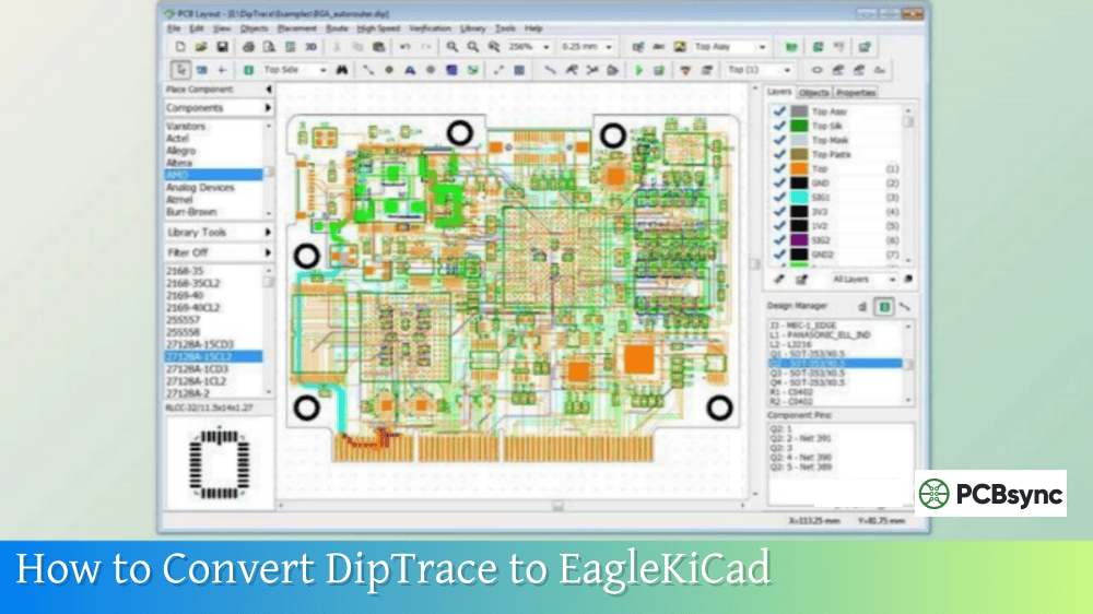
How to Convert DipTrace Files to Altium, Eagle & KiCad
Switching between PCB design tools is a reality for most engineers. Whether you’re collaborating with teams using different software, inheriting projects from other designers, or migrating to a new platform, knowing how to convert DipTrace files to other formats saves countless hours of redrawing. This guide covers practical methods for DipTrace to Altium, DipTrace to Eagle, and DipTrace to KiCad conversion.
Before attempting any conversion, understand what DipTrace can export natively. DipTrace version 5 supports extensive import/export options across schematics, PCB layouts, and component libraries.
The key to successful conversion is identifying which intermediate format works best for your target software.
Converting DipTrace to Altium Designer
DipTrace to Altium conversion uses P-CAD ASCII as the bridge format. Altium can import P-CAD files through its Import Wizard, making this the most reliable path.
Step-by-Step PCB Layout Conversion
In DipTrace PCB Layout:
Open your completed PCB design (.dip file)
Go to File → Export → P-CAD ASCII
Save the file with .pcb extension
Repeat for any associated schematic files
In Altium Designer:
Launch Altium and select File → Import Wizard
Choose “P-CAD Designs and Libraries” as the source
Select the P-CAD ASCII files you exported
Follow the wizard to specify output locations
Review and complete the import
Schematic Conversion Considerations
Schematic DipTrace to Altium conversion has some limitations. Users report that wire connections sometimes don’t transfer correctly—components appear but some nets show as unconnected.
Workarounds:
Export netlist from DipTrace separately
Manually verify net connectivity after import
Use the PCB layout as reference to fix schematic connections
Library Conversion
Converting component libraries requires extra steps because DipTrace and Altium handle footprint-to-symbol associations differently.
The Issue: In DipTrace, patterns are embedded within component libraries. Altium keeps schematic symbols and PCB footprints in separate files.
Solution:
Export schematic library to P-CAD V16 format (.lia)
Export pattern library to P-CAD V16 format (.lia)
Import both files separately into Altium
Manually attach footprints to schematic symbols in Altium
Known Issues and Fixes
Problem
Cause
Solution
File format error
Binary vs ASCII format
Ensure DipTrace exports ASCII, not binary
Missing connections
Net label translation issues
Manually reconnect using exported netlist
Overlay text displaced
Formatting differences
Adjust text positions in Altium after import
Scaled incorrectly
Unit mismatch
Verify units match (mil, mm) before export
Converting DipTrace to Eagle
DipTrace to Eagle conversion is more limited because DipTrace doesn’t export directly to Eagle format. However, several methods exist.
Method 1: Eagle Board Export (Direct)
DipTrace can export PCB layouts directly to Eagle board format:
This method works for PCB layouts but doesn’t include schematic data.
Method 2: Schematic via Eagle XML
For schematics, DipTrace exports to Eagle Schematic format:
Open schematic in DipTrace Schematic Capture
File → Export → Eagle Schematic
Import the resulting file into Eagle
Method 3: Using Netlists
When direct conversion fails, use netlist export as a bridge:
Export PCB netlist from DipTrace (File → Export → Netlist)
Import the netlist into Eagle
Place components manually and use the netlist for connectivity
Limitations of DipTrace to Eagle Conversion
DipTrace to Eagle conversion faces challenges because Eagle’s format is proprietary and not fully documented. The DipTrace forum shows years of user requests for better Eagle export support.
What Works
What Doesn’t Work Well
Basic board outlines
Complex copper pours
Component placement
Custom pad shapes
Simple routing
Multi-layer designs
Standard footprints
Custom components
Reverse Direction: Eagle to DipTrace
If you need to go from Eagle to DipTrace (useful for collaboration), DipTrace includes ULP scripts in the Utils folder:
Open Eagle and load your schematic or board
Click the ULP button
Navigate to C:\Program Files\DipTrace\Utils
Select Eagle_to_DipTrace_SCH.ulp or Eagle_to_DipTrace_BRD.ulp
Save the resulting ASCII file
Import into DipTrace via File → Import → DipTrace ASCII
Note: These scripts work best with Eagle versions 7.2 and earlier. Newer Eagle versions may produce compatibility issues.
Converting DipTrace to KiCad
DipTrace to KiCad conversion has improved significantly in recent DipTrace versions, which now support direct KiCad format export.
DipTrace exports directly to KiCad footprint format:
Open Pattern Editor
Select Library → Export → KiCad Footprints
Choose the .kicad_mod output folder
Import into KiCad Footprint Editor
Known DipTrace to KiCad Issues
Users report reference designator swapping during schematic import—components like JP1, JP2, JP3 may become JP3, JP1, JP2. This causes mismatch errors when linking schematic to PCB.
Solutions:
Verify reference designators match between schematic and PCB after import
Use “Update PCB from Schematic” in KiCad to re-establish connections
Manually correct any mismatches before routing
Using Intermediate Formats for Complex Conversions
When direct conversion fails, intermediate formats provide alternative paths.
PADS format provides another bridge, especially useful for Mentor Graphics tools:
DipTrace exports PADS PCB ASCII 2005 format
PADS can open these files directly
From PADS, export to other formats as needed
One useful workaround: if you have PADS PCB version 9.3 or higher, you can open Altium schematics directly, export as PADS 2005 format, then import to DipTrace. This provides an indirect path when direct Altium-to-DipTrace conversion fails.
Netlist-Based Transfer
When visual layout preservation isn’t critical, netlist transfer ensures electrical connectivity:
Supported Netlist Formats:
Accel
Allegro
KiCad
Mentor
OrCAD
PADS
P-CAD
Protel 2.0
Tango
Export the netlist, import into target software, place components, and route fresh. This guarantees electrical correctness even if layout needs recreation.
Advanced Conversion Scenarios
Converting Multi-Sheet Hierarchical Designs
Hierarchical schematics present additional challenges during conversion. DipTrace’s hierarchical block structure may not translate directly to other tools’ hierarchy implementations.
Recommended approach:
Flatten the hierarchy in DipTrace before export if possible
Export each sheet separately
Rebuild hierarchy structure in target software
Verify inter-sheet connections using exported netlist
Handling Differential Pairs and High-Speed Constraints
Design rules, differential pair definitions, and length-matching constraints typically don’t survive conversion between tools. These are software-specific features that must be recreated manually.
After conversion, you’ll need to:
Redefine differential pairs in the target tool
Re-enter length matching rules
Reconfigure impedance calculations based on new stackup definitions
Verify trace routing still meets original specifications
Converting Copper Pours and Planes
Copper pour conversion varies significantly between tools. Some conversions successfully transfer pour definitions while others lose them entirely, leaving ratlines where plane connections existed.
Target Tool
Copper Pour Status
Altium (via P-CAD)
Usually preserved, verify net assignments
Eagle
May convert as solid regions, verify connectivity
KiCad
Generally works, check thermal relief settings
Always verify ground and power plane integrity after conversion by running a design rule check and confirming no open connections exist.
Binary vs ASCII File Formats
A common conversion failure occurs when attempting to import binary files instead of ASCII versions. Both Altium’s .SchDoc and .PcbDoc files can exist in either format with identical extensions.
How to verify file format:
Open the file in a text editor (Notepad, VS Code)
ASCII files show readable text at the beginning
Binary files show garbled characters
If you receive “Wrong file format” errors during import, the source file is likely binary. Open it in the original software and save/export as ASCII format.
Can I convert DipTrace files directly to Altium format?
Not directly. DipTrace to Altium conversion requires using P-CAD ASCII as an intermediate format. Export from DipTrace to P-CAD ASCII, then use Altium’s Import Wizard to bring the files in. PCB layouts convert reasonably well, but schematic wiring may need manual verification and repair after import.
Why don’t my Eagle exports include schematics?
DipTrace to Eagle export for schematics uses Eagle Schematic format (File → Export → Eagle Schematic), which is separate from board export. You need to export the schematic and board as two separate files, then link them in Eagle. Some complex designs may require netlist-based reconstruction rather than direct conversion.
Does DipTrace support direct KiCad export?
Yes, DipTrace version 5 supports direct DipTrace to KiCad export for both PCB layouts (File → Export → KiCad Board) and netlists. Footprint libraries can also be exported directly to KiCad format through Pattern Editor. However, schematic symbol libraries require netlist-based transfer rather than direct format conversion.
What’s the best format for preserving design integrity during conversion?
P-CAD ASCII format generally preserves the most design information when converting between professional EDA tools. It captures component placement, routing, net names, and layer assignments. However, complex features like differential pair definitions, custom design rules, and embedded 3D models may not transfer completely and require manual recreation.
Why do reference designators change during conversion?
Reference designator mismatches occur because different EDA tools store component relationships differently. DipTrace uses internal IDs that map to RefDes names, while other tools may sort components differently during import. Always verify RefDes assignments after import by comparing against your original design, and use the target software’s annotation tools to correct any mismatches before proceeding with modifications.
Conclusion
Converting DipTrace files to other EDA platforms requires understanding both the source and target software formats. DipTrace to Altium works best through P-CAD ASCII, DipTrace to Eagle uses direct board export or ULP scripts for reverse direction, and DipTrace to KiCad benefits from DipTrace’s native KiCad export support.
No conversion is perfect. Budget time for verification and manual fixes, especially for complex designs with custom components. When precise layout preservation matters, consider maintaining parallel projects in both tools rather than relying entirely on conversion.
The effort invested in understanding these conversion workflows pays dividends when collaborating across teams or transitioning between platforms. Keep original files archived, document any manual modifications required, and verify electrical connectivity thoroughly before manufacturing converted designs.
Inquire: Call 0086-755-23203480, or reach out via the form below/your sales contact to discuss our design, manufacturing, and assembly capabilities.
Quote: Email your PCB files to Sales@pcbsync.com (Preferred for large files) or submit online. We will contact you promptly. Please ensure your email is correct.
Notes: For PCB fabrication, we require PCB design file in Gerber RS-274X format (most preferred), *.PCB/DDB (Protel, inform your program version) format or *.BRD (Eagle) format. For PCB assembly, we require PCB design file in above mentioned format, drilling file and BOM. Click to download BOM template To avoid file missing, please include all files into one folder and compress it into .zip or .rar format.


