Inquire: Call 0086-755-23203480, or reach out via the form below/your sales contact to discuss our design, manufacturing, and assembly capabilities.
Quote: Email your PCB files to Sales@pcbsync.com (Preferred for large files) or submit online. We will contact you promptly. Please ensure your email is correct.
Notes: For PCB fabrication, we require PCB design file in Gerber RS-274X format (most preferred), *.PCB/DDB (Protel, inform your program version) format or *.BRD (Eagle) format. For PCB assembly, we require PCB design file in above mentioned format, drilling file and BOM. Click to download BOM template To avoid file missing, please include all files into one folder and compress it into .zip or .rar format.
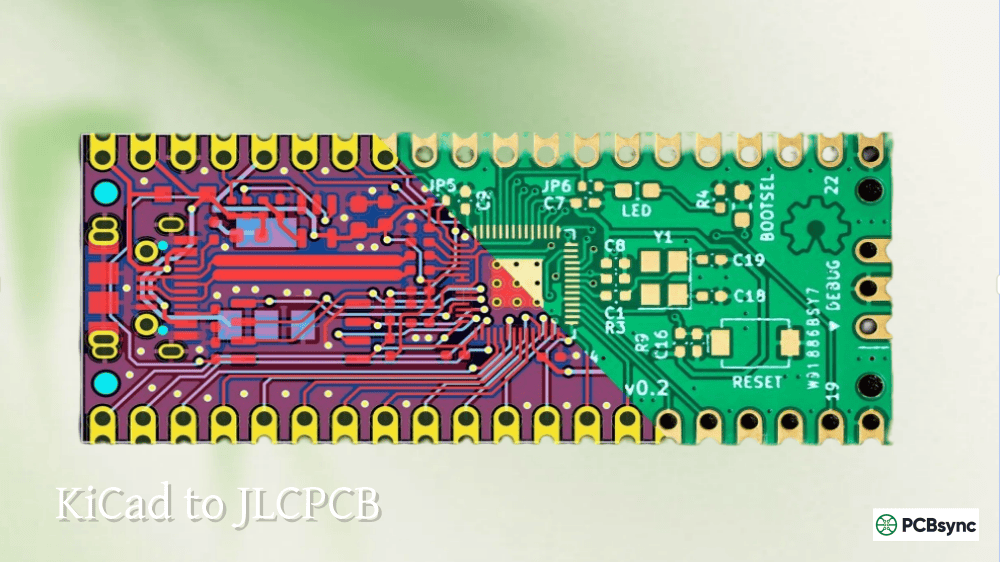
Getting your KiCad design manufactured should be the exciting finish line of a project, not a frustrating exercise in file format troubleshooting. Yet the number of forum posts asking “why won’t JLCPCB accept my Gerbers?” or “what settings does PCBWay need?” suggests many designers struggle with this final step.
The reality is that each PCB manufacturer has slightly different preferences for Gerber settings, drill file formats, and assembly file requirements. What works perfectly for JLCPCB KiCad exports might cause issues at OSHPark or Eurocircuits. This guide covers the exact export settings for the most popular fabrication houses, from budget-friendly Chinese manufacturers to premium European and American options.
Whether you’re ordering bare boards from PCBWay KiCad projects or getting full assembly from JLCPCB, understanding these manufacturer-specific requirements saves time, money, and the frustration of rejected orders or incorrectly manufactured boards.
Pre-Export Checklist: KiCad DRC and Design Verification
Before generating any manufacturing files, running a thorough Design Rule Check prevents the majority of fabrication issues. The KiCad JLCPCB DRC process catches problems that would otherwise result in rejected orders or boards that don’t work.
Running DRC in KiCad
Open your PCB in the PCB Editor
Go to Inspect → Design Rules Checker (or press the DRC icon)
Click “Run DRC”
Fix all errors before proceeding
Review warnings individually (some may be acceptable)
Critical Pre-Export Steps
Step
Why It Matters
Run DRC
Catches clearance violations, unconnected nets
Refill zones (press B)
Ensures copper pours reflect current design
Check zone fills before plotting
KiCad prompts if zones are outdated
Update board from schematic
Syncs any last-minute changes
Verify mounting holes
Confirm NPTH vs PTH settings
Zone fills are particularly important. If you’ve made routing changes since the last zone fill, your Gerbers won’t match your intended design. KiCad can prompt you during export, but catching this earlier avoids confusion.
Understanding Gerber Files and What Manufacturers Need
Gerber files are the industry standard for PCB manufacturing data. Each layer of your design becomes a separate Gerber file, and together with drill files, they provide everything a manufacturer needs to fabricate your board.
For four-layer boards, add In1.Cu and In2.Cu to your export. Six-layer designs need In1.Cu through In4.Cu.
Protel vs KiCad Filename Extensions
Most manufacturers prefer Protel filename extensions (.GTL, .GBL, etc.) over KiCad’s default naming. The “Use Protel filename extensions” checkbox in the Plot dialog handles this automatically. While modern fab houses can usually identify KiCad’s native filenames, using Protel extensions reduces the chance of layer misidentification.
JLCPCB KiCad Export Settings
JLCPCB is arguably the most popular choice for hobbyist and prototype PCB manufacturing. Their JLCPCB KiCad documentation is comprehensive, but here are the exact settings that work reliably.
Gerber Settings for JLCPCB
Open File → Fabrication Outputs → Gerbers (.gbr) and configure:
For SMT assembly service, JLCPCB requires BOM and CPL (Component Placement List) files in specific formats.
BOM File Requirements:
Comment (part description/value)
Designator (C1, R1, U1, etc.)
Footprint (package size)
LCSC Part Number (optional but recommended)
CPL File Requirements:
Designator
Mid X, Mid Y coordinates
Rotation
Layer (Top/Bottom)
The easiest approach is using the kicad-jlcpcb-tools plugin (github.com/Bouni/kicad-jlcpcb-tools), which generates correctly formatted files with one click and includes LCSC part number lookup.
Manual CPL Generation:
Go to File → Fabrication Outputs → Footprint Position (.pos) File
Format: CSV
Units: Millimeters
Files: Separate files for front and back
Note that JLCPCB requires specific column headers. The plugin handles this, but manual files may need header renaming.
PCBWay KiCad Export Settings
PCBWay offers similar services to JLCPCB with slightly different preferences. The KiCad PCBWay workflow benefits from their dedicated plugin that automates the entire process.
Using the PCBWay Plugin for KiCad
PCBWay provides an official plugin (github.com/pcbway/PCBWay-Plug-in-for-Kicad) that exports files and opens their ordering page directly:
Install via Plugin and Content Manager
Click the PCBWay button in PCB Editor
Files are automatically generated and uploaded
Complete your order on the PCBWay website
Manual Gerber Export for PCBWay
If you prefer manual export, use these settings:
Gerber Options:
Use Protel filename extensions: Checked
Do NOT check “Use extended X2 format” (PCBWay historically has issues with X2)
Coordinate format: 4.6
Drill Settings:
Suppress leading zeros: Checked
Minimal header: Checked
Drill Units: Millimeters
Important PCBWay Note: Their documentation explicitly states not to use extended X2 format for Gerbers. While many modern manufacturers support X2, PCBWay’s CAM system works better with standard RS-274X format.
PCBWay Assembly Files
For assembly orders, PCBWay needs:
BOM in CSV format
Position file (Footprint Position output from KiCad)
The position file works directly from KiCad’s output without modification in most cases.
OSHPark KiCad Settings and Native File Upload
OSHPark stands out by accepting native .kicad_pcb files directly. This eliminates Gerber generation entirely for OSHPark KiCad users.
Direct KiCad Upload to OSHPark
Simply upload your .kicad_pcb file to oshpark.com. Their system:
Processes the file using KiCad 9.x internally
Generates Gerbers on their end
Shows a preview for verification
Advantages:
No Gerber generation needed
Fewer opportunities for export errors
Simpler workflow for beginners
Considerations:
Zone fills must be up to date (OSHPark doesn’t refill zones)
Custom fonts may render differently (embed fonts in KiCad 9+)
Design rules from .kicad_pro aren’t included
Gerber Export for OSHPark
If you prefer uploading Gerbers (for verification or using older KiCad versions):
Critical Settings:
Uncheck “Plot sheet reference on all layers” (causes board size detection issues)
Check “Exclude PCB Edge from other layers”
Use Protel filename extensions: Recommended but not required
Drill Settings:
Excellon format
Decimal format for zeros
Millimeters or inches both work
OSHPark’s system is notably flexible with file formats and will detect KiCad-generated files automatically.
Aisler KiCad Integration (European Manufacturer)
Aisler KiCad integration is exceptionally smooth for European designers wanting local manufacturing. Like OSHPark, Aisler accepts native KiCad files.
Aisler Push for KiCad Plugin
The official plugin (github.com/AislerHQ/PushForKiCad) provides one-click ordering:
For assembly services, add MPN (Manufacturer Part Number) fields to schematic symbols. Aisler reads these directly for component sourcing.
Eurocircuits KiCad Settings (European Premium)
Eurocircuits KiCad support includes native file upload and comprehensive DRC guidelines. As a premium European manufacturer, they offer tight tolerances and excellent quality.
Native KiCad File Upload
Eurocircuits accepts .kicad_pcb files directly through their PCB Visualizer, which provides immediate DFM feedback before ordering.
Eurocircuits provides downloadable DRC settings for various CAD packages, though KiCad requires manual entry in Board Setup → Design Rules.
AllPCB KiCad Export Considerations
AllPCB KiCad users should note some specific requirements, particularly for assembly services.
Assembly File Requirements
AllPCB requires additional layers for assembly:
Fabrication layers with component designators
BOM in XLSX format (not CSV)
Position file with specific column formatting
Export Fabrication Layers: Check F.Fab and B.Fab in your Gerber export if using assembly services. These layers show component outlines and reference designators that help assembly staff.
Gerber Settings
Standard settings work for bare board orders:
Use Protel filename extensions
Excellon drill format
Decimal zeros format
PCB Manufacturer Comparison Table
Manufacturer
Native KiCad
Plugin
Typical 2-Layer Price
Lead Time
Assembly
JLCPCB
No
Yes (community)
$2-5
3-7 days
Yes
PCBWay
No
Yes (official)
$5-10
3-7 days
Yes
OSHPark
Yes
No
$5/sq inch
12+ days
No
Aisler
Yes
Yes (official)
€12+
1-7 days
Yes
Eurocircuits
Yes
No
€30+
2-7 days
Yes
AllPCB
No
No
$5-15
3-7 days
Yes
NextPCB
No
No
$2-5
3-7 days
Yes
Prices are approximate for small prototype quantities and vary based on specifications.
KiCad Fabrication Plugins and Tools
Several plugins streamline the export process for specific manufacturers.
Always verify your exported Gerbers before uploading. Catching errors at this stage is free; catching them after manufacturing is expensive.
Free Gerber Viewers
Tool
Platform
Notes
KiCad GerbView
Cross-platform
Built into KiCad
Gerbv
Linux/Windows
Lightweight, fast
Gerblook.org
Web
Quick online check
JLCPCB Gerber Viewer
Web
Shows what JLCPCB will manufacture
PCBWay Gerber Viewer
Web
Included in order process
Verification Checklist
Check
What to Look For
Layer alignment
All layers registered correctly
Drill holes
Present and correctly sized
Board outline
Closed path, correct dimensions
Silkscreen
No text on pads, readable size
Solder mask
Correct pad exposure
Copper connections
No unintended shorts/opens
Configuring KiCad DRC for Different Manufacturers
Each manufacturer has different minimum specifications. Setting up the correct KiCad JLCPCB DRC rules before starting your layout prevents costly redesigns.
Setting Design Rules in KiCad
Go to File → Board Setup → Design Rules to configure constraints:
Constraints Tab:
Minimum clearance
Minimum track width
Minimum connection width
Minimum annular ring
Pre-defined Sizes Tab:
Track widths
Via sizes
Differential pair dimensions
Manufacturer-Specific DRC Settings
Parameter
JLCPCB
PCBWay
OSHPark
Eurocircuits
Min Track
0.127mm (5mil)
0.1mm (4mil)
0.152mm (6mil)
0.15mm
Min Space
0.127mm (5mil)
0.1mm (4mil)
0.152mm (6mil)
0.15mm
Min Via Hole
0.3mm
0.3mm
0.254mm (10mil)
0.2mm
Min Via Diameter
0.5mm
0.5mm
0.508mm (20mil)
0.45mm
Min Annular Ring
0.13mm
0.1mm
0.127mm
0.125mm
These represent standard service levels. Tighter tolerances are available at higher prices.
Creating Manufacturer Templates
Create separate KiCad project templates for each manufacturer:
Set up a new project with correct design rules
Configure the Plot dialog settings
Save as template via File → New Project from Template → Save Current Project as Template
This ensures consistent export settings across all projects targeting that manufacturer.
Common Export Problems and Solutions
Missing Drill Holes
Symptom: Manufacturer reports no drill file or missing holes Solution: Always click “Generate Drill Files” separately after plotting Gerbers. It’s a separate step that’s easy to forget.
Board Outline Not Detected
Symptom: Quote shows wrong dimensions or upload fails Solution:
Ensure Edge.Cuts layer contains a closed path
Check for small gaps in the outline
Remove any non-outline elements from Edge.Cuts
Zone Fills Outdated
Symptom: Copper pours don’t match expected design Solution: Press B to refill zones before export, or enable “Check zone fills before plotting”
Component Rotation Issues (Assembly)
Symptom: Parts placed at wrong angles in assembly preview Solution: The kicad-jlcpcb-tools plugin includes rotation correction. For manual files, edit the rotation column in the CPL file.
Silkscreen on Pads
Symptom: Manufacturer removes silkscreen unexpectedly Solution: Enable “Subtract soldermask from silkscreen” in Gerber options
Can I upload .kicad_pcb files directly to JLCPCB instead of Gerbers?
No, JLCPCB requires Gerber files. Unlike OSHPark and Aisler, JLCPCB’s system doesn’t process native KiCad files. Use the standard export process or the JLCPCB Tools plugin to generate the required files. The plugin automates everything and produces correctly formatted Gerbers, BOM, and CPL files.
Why does KiCad’s default Gerber export not work with PCBWay?
KiCad’s defaults are generally compatible, but PCBWay specifically recommends not using “Extended X2 format” for Gerbers. Their CAM system processes standard RS-274X format more reliably. Also ensure “Use Protel filename extensions” is checked for easier layer identification.
What’s the difference between JLCPCB’s BOM and CPL files?
The BOM (Bill of Materials) lists what components go on the board with values, footprints, and part numbers. The CPL (Component Placement List, also called centroid or pick-and-place file) specifies where each component goes with X/Y coordinates, rotation, and which side of the board. Both are required for assembly services.
Should I use Gerber X2 format or standard RS-274X?
For JLCPCB and most Asian manufacturers, standard RS-274X works most reliably. For Eurocircuits and some European fabs, Gerber X2/X3 provides additional metadata that improves DFM checking. When in doubt, RS-274X (don’t check “Use extended X2 format”) is the safer choice. OSHPark and Aisler handle either format well through their native file processing.
How do I fix component rotation errors in JLCPCB assembly preview?
JLCPCB’s system expects certain rotation conventions that may differ from KiCad’s output. The kicad-jlcpcb-tools plugin includes a rotation correction database that automatically adjusts common footprints. For manual correction, edit the Rotation column in your CPL file. The plugin also has a Rotation Manager where you can add custom corrections for footprints not in the database.
Streamlining Your KiCad Manufacturing Workflow
The key to smooth PCB ordering is establishing a consistent workflow. Once you’ve configured export settings for your preferred manufacturer, save them as part of your project template. The community plugins for JLCPCB and PCBWay dramatically reduce friction by handling all the formatting details automatically.
Recommended Workflow Steps
Design Phase: Use manufacturer DRC settings from the start
Pre-Export: Run DRC, refill zones, update from schematic
Export: Use plugin or manual settings for target manufacturer
Verify: Check Gerbers in GerbView or online viewer
Upload: Submit to manufacturer and verify preview
Review: Check manufacturer’s DFM feedback before confirming
Cost Optimization Tips
When ordering from multiple manufacturers, consider:
JLCPCB KiCad Projects: Best for high-volume prototypes with assembly needs. Their parts library is extensive, and basic boards start at $2.
PCBWay KiCad Orders: Similar pricing to JLCPCB with occasionally better options for special finishes like gold fingers or heavy copper.
OSHPark KiCad Designs: Premium purple boards, excellent for US-based designers wanting simpler ordering. Cost scales with board size rather than fixed minimum orders.
Aisler KiCad Users: Ideal for European designers. Local manufacturing means faster delivery without customs hassles.
Eurocircuits KiCad Projects: When quality and precision matter more than cost. Excellent for high-reliability applications.
For beginners, OSHPark and Aisler’s native KiCad file support eliminates the Gerber learning curve entirely. Upload your board file, verify the preview, and order. As you gain experience, the flexibility of Gerber exports lets you shop around between manufacturers for the best combination of price, quality, and turnaround time.
Remember that every manufacturer’s engineers want your order to succeed. When in doubt about settings, their support teams are generally responsive and helpful. But with the correct export settings from this guide, most orders should process without any manual intervention.
Inquire: Call 0086-755-23203480, or reach out via the form below/your sales contact to discuss our design, manufacturing, and assembly capabilities.
Quote: Email your PCB files to Sales@pcbsync.com (Preferred for large files) or submit online. We will contact you promptly. Please ensure your email is correct.
Notes: For PCB fabrication, we require PCB design file in Gerber RS-274X format (most preferred), *.PCB/DDB (Protel, inform your program version) format or *.BRD (Eagle) format. For PCB assembly, we require PCB design file in above mentioned format, drilling file and BOM. Click to download BOM template To avoid file missing, please include all files into one folder and compress it into .zip or .rar format.


