Inquire: Call 0086-755-23203480, or reach out via the form below/your sales contact to discuss our design, manufacturing, and assembly capabilities.
Quote: Email your PCB files to Sales@pcbsync.com (Preferred for large files) or submit online. We will contact you promptly. Please ensure your email is correct.
Notes: For PCB fabrication, we require PCB design file in Gerber RS-274X format (most preferred), *.PCB/DDB (Protel, inform your program version) format or *.BRD (Eagle) format. For PCB assembly, we require PCB design file in above mentioned format, drilling file and BOM. Click to download BOM template To avoid file missing, please include all files into one folder and compress it into .zip or .rar format.
If you’ve spent any time researching PCB design software, you’ve probably stumbled across KiCad. Maybe you’re tired of paying thousands for Altium licenses, or perhaps you’ve outgrown the limitations of EAGLE’s free tier. Whatever brought you here, I’m going to walk you through everything you need to know about KiCad EDA in 2026.
I’ve been designing boards professionally for over a decade, and I’ve watched KiCad evolve from a clunky open-source project into a legitimate powerhouse that rivals commercial tools costing thousands of dollars. Let me share what I’ve learned.
KiCad is a free, open-source Electronic Design Automation (EDA) software suite used for creating schematics and designing printed circuit boards. Originally created by Jean-Pierre Charras in 1992 at IUT de Grenoble, the software has grown into one of the most capable PCB design tools available today.
The name “KiCad” comes from combining the first letters of a company name belonging to Jean-Pierre’s friend with the term “CAD.” While the origins might be humble, the software has matured dramatically over three decades of development.
What makes KiCad stand out in 2026 is its combination of professional-grade features and zero licensing costs. Unlike commercial alternatives that charge hundreds or thousands annually, KiCad offers unlimited board sizes, unlimited layers, and no restrictions on commercial use. The current stable version, KiCad 9, represents the culmination of years of development supported by organizations like CERN, the Raspberry Pi Foundation, and Digi-Key Electronics.
Why KiCad Free Beats Many Paid Alternatives
Here’s what genuinely surprised me when I first switched to KiCad from a commercial tool: the feature set isn’t just “good enough” for free software. It’s genuinely competitive with professional-grade applications.
No Artificial Limitations
Most free PCB software comes with strings attached. Limited board sizes. Restricted layer counts. Mandatory use of specific manufacturers. KiCad has none of that. You get the full application with every feature unlocked from day one. There are no “standard,” “premium,” or “platinum” versions to navigate.
Professional-Grade Routing Tools
The interactive router in KiCad supports push-and-shove routing, which automatically moves existing traces out of the way as you route new ones. You also get differential pair routing for high-speed signals and length-tuning tools for matching trace lengths in DDR or other timing-critical designs.
Comprehensive Design Rule Checking
KiCad’s DRC engine lets you define custom rules for clearances, trace widths, via sizes, and more. In version 9, you can even write custom DRC expressions for complex design requirements that standard rule sets can’t capture.
Native SPICE Simulation
The integrated ngspice simulator lets you verify circuit behavior before you ever commit to a layout. You can run AC analysis, DC sweeps, transient simulations, and more without leaving the KiCad environment.
KiCad EDA Core Features Breakdown
Understanding what’s included in the KiCad EDA suite helps you appreciate its capabilities. The software isn’t just one application but a collection of tightly integrated tools.
Schematic Editor (Eeschema)
The schematic capture environment supports everything from simple single-sheet designs to complex hierarchical projects with dozens of interconnected sheets. Key capabilities include:
Hierarchical sheet support for organized, modular designs
Electrical Rules Check (ERC) for catching connection errors
Bus support for grouping related signals
Custom symbol creation and editing
Annotation tools for automatic reference designator assignment
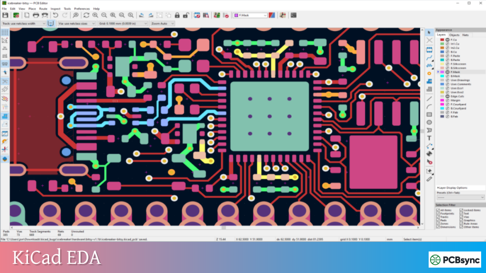
PCB Layout Editor (Pcbnew)
This is where your schematic becomes a physical board. The PCB editor includes:
Support for up to 32 copper layers
Interactive routing with collision detection
Push-and-shove routing mode
Differential pair routing
Length tuning for matched impedance designs
Zone fills for ground planes and power planes
Comprehensive DRC with custom rule support
3D Viewer
KiCad’s 3D viewer lets you inspect your board design from every angle. This isn’t just eye candy—it’s genuinely useful for:
Checking component clearances
Verifying mechanical fit before manufacturing
Creating renders for documentation
Exporting STEP files for mechanical CAD integration
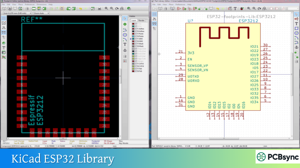
Symbol and Footprint Editors
Creating custom components is straightforward with dedicated editors for both schematic symbols and PCB footprints. The tools support:
Multiple unit symbols (like a quad op-amp)
Complex pad shapes and custom outlines
3D model assignment for visualization
Library management across projects
Getting Started: KiCad Website and Download
You can download KiCad from the official website at kicad.org. The KiCad website provides installers for Windows, macOS, and Linux, along with comprehensive documentation and community resources.
The installation typically includes the full official component library, which contains thousands of symbols, footprints, and 3D models. Most users can start designing immediately without downloading additional libraries.
KiCad 9: What’s New in the Latest Version
KiCad 9.0, released in February 2025, brought significant improvements across the entire design workflow. If you’re upgrading from an earlier version or just starting out, here’s what you need to know.
Output Jobsets
One of the most requested features, jobsets let you define automated output generation. Instead of manually exporting Gerbers, drill files, BOMs, and PDFs every time you revise a design, you create a jobset once and run it with a single click. This is a massive time-saver for production workflows.
Zone Manager
The new Zone Manager provides centralized control over all copper zones in your design. You can view, edit, and organize zones from a dedicated panel instead of hunting through the board for each one. For complex multi-layer designs with numerous power planes, this feature alone justifies the upgrade.
Design Blocks
Design blocks allow you to create reusable schematic sections. If you frequently use the same power supply circuit, sensor interface, or protection circuit, you can save it as a block and drop it into future projects. Layout block support is planned for future versions.
Improved 3D Model Export
The 3D export system received significant updates, making it easier to generate accurate STEP models for mechanical integration. The raytracer also saw improvements for more realistic renders.
Additional Improvements
Sheet pin and hierarchical label synchronization tool
Schematic net class rule areas
Component classes for grouping and management
Enhanced selection filtering in all editors
ODB++ export support
Git integration for version control
KiCad Commercial Use: What You Need to Know
One of the most common questions I hear is whether KiCad is actually free for commercial use. The answer is unambiguously yes.
The GPL v3 License Explained
KiCad is licensed under the GNU General Public License version 3 (GPL v3). This license explicitly permits commercial use. You can use KiCad to design products you sell, create boards for clients, or run a design consultancy without paying Anthropic or anyone else a licensing fee.
The GPL doesn’t restrict how you use the software—it restricts how you distribute the software. If you modify KiCad’s source code and distribute your modified version, you must make your changes available under the same license. But if you’re just using KiCad to design boards, this doesn’t apply to you at all.
Library Licensing
The KiCad official libraries use a Creative Commons CC-BY-SA 4.0 license with a special exception. This means you can use the library components in your commercial designs without any attribution requirements or licensing concerns. The exception specifically states that using library data in a project does not require you to share your project files.
Real-World Commercial Adoption
Numerous companies use KiCad for production designs. Olimex, a well-known electronics manufacturer, publicly switched from EAGLE to KiCad in 2015 and has used it for all their products since. Many startups, small businesses, and even departments within larger companies have adopted KiCad to reduce software costs without sacrificing capability.
KiCad Professional Use: Is It Ready for Serious Work?
This is where I’ll be direct: KiCad is absolutely ready for professional use in 2026. The gap between KiCad and commercial tools like Altium has narrowed dramatically.
Where KiCad Excels
KiCad handles the following professional requirements without issue:
Multi-layer boards up to 32 layers
Complex hierarchical schematics
High-density layouts with fine-pitch components
Differential pair routing for USB, HDMI, and similar interfaces
Length matching for DDR memory interfaces
Design rule checking with custom constraints
Standard manufacturing outputs (Gerber, drill files, pick-and-place)
Honest Limitations
KiCad isn’t perfect for every use case. Here’s where you might still need a commercial tool:
Real-time team collaboration: Altium 365 offers cloud-based collaboration that KiCad can’t match. KiCad does support Git, but it’s not the same as simultaneous editing.
Integrated supply chain tools: Commercial tools often include real-time pricing, availability checking, and lifecycle status integrated into the schematic editor.
Advanced simulation: While KiCad includes SPICE simulation, dedicated tools like OrCAD PSpice offer more advanced analysis capabilities.
Formal documentation: Some regulated industries require specific documentation formats that commercial tools generate more readily.
Making the Decision
For most professional applications—prototypes, small-batch production, consumer electronics, industrial controls—KiCad handles everything you need. The main reasons to choose commercial software in 2026 are team collaboration requirements, regulatory compliance in aerospace or medical devices, or legacy workflows built around specific tools.
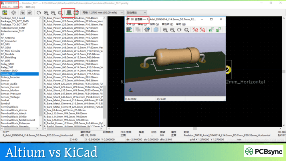
KiCad vs. Altium vs. EAGLE: Quick Comparison
Feature
KiCad
Altium Designer
EAGLE
Cost
Free
~$7,000/year
$100-500/year
Layer limit
32
Unlimited
2-16 (varies by tier)
Board size limit
~2.1m
Unlimited
Limited in free version
3D modeling
Yes
Yes (advanced)
Yes
Push-and-shove routing
Yes
Yes
Limited
SPICE simulation
Yes (integrated)
Yes (advanced)
No
Real-time collaboration
Git-based
Cloud-based
Git-based
Learning curve
Moderate
Steep
Easy
Commercial use
Yes
Yes
Yes (paid versions)
Autorouter
External (FreeRouting)
Built-in
Built-in
Essential KiCad Resources and Library Downloads
Building an efficient KiCad workflow means knowing where to find components, tutorials, and help when you need it.
Effective library management separates efficient designers from frustrated ones. KiCad’s library system is flexible but requires understanding to use effectively.
Library Types and Organization
KiCad uses separate libraries for symbols (schematic representations) and footprints (physical PCB patterns). These are intentionally decoupled, allowing one symbol to work with multiple footprints. A generic resistor symbol can connect to 0402, 0603, 0805, or through-hole footprints depending on your needs.
Global libraries are available to all projects and typically include the official KiCad libraries installed with the software. Project libraries live within specific projects and contain custom or modified components for that design only.
Building a Personal Library Strategy
I recommend a three-tier approach:
Tier 1: Official libraries. Use official KiCad libraries for common components like basic passives, common ICs, and standard connectors. These are well-maintained and regularly updated.
Tier 2: Curated third-party libraries. Download libraries from trusted sources like Digi-Key or SnapMagic for specific components not in the official collection. Keep these in a personal library folder that you back up and version control.
Tier 3: Custom components. Create your own symbols and footprints only when necessary. Follow KiCad library conventions to ensure compatibility and maintainability.
Creating Custom Footprints
When you need a footprint that doesn’t exist, the Footprint Editor makes creation straightforward. Start with a similar existing footprint when possible—modifying an SOIC-8 to create an SOIC-14 is faster than starting from scratch.
Always verify footprints against manufacturer datasheets. Pay attention to:
Pad dimensions and spacing
Courtyard size for assembly equipment
Silkscreen markings for orientation
3D model alignment
Test new footprints by printing your layout at 1:1 scale and placing actual components on the paper. This simple check catches sizing errors before you order boards.
Managing Library Updates
The official KiCad libraries receive regular updates with bug fixes and new components. However, updating mid-project can cause issues if library components change. My approach:
Start new projects with the current library version
Don’t update libraries on in-progress designs unless necessary
If you must update, verify all components still resolve correctly
Keep project-specific copies of critical components as a fallback
Advanced KiCad Features Worth Learning
Once you’re comfortable with basic operation, these advanced features significantly improve productivity.
Custom Design Rules
KiCad 9’s custom DRC rules let you encode complex requirements that standard settings can’t express. For example, you might require extra clearance between specific net classes, mandate minimum copper width on power nets, or enforce different rules on inner versus outer layers.
The rule syntax takes some learning, but the capability is powerful:
For high-speed interfaces like DDR memory, USB, or HDMI, signal timing depends on matched trace lengths. KiCad’s length tuning tools let you add serpentine patterns to shorter traces, bringing them to the same electrical length as longer routes.
Access length tuning through the Route menu or by pressing the length tuning shortcut during routing. The tool shows real-time length information and guides you to achieve your matching targets.
Differential Pair Routing
High-speed differential signals (USB, LVDS, Ethernet) require paired traces with controlled impedance and tight coupling. KiCad’s differential pair router handles these automatically, maintaining the pair relationship while you focus on the route path.
Configure differential pair settings in your net class definitions, specifying track width, spacing, and via handling for each pair.
Scripting and Automation
KiCad includes Python scripting support, enabling automation of repetitive tasks. You can write scripts to:
Generate component arrays programmatically
Export custom reports and documentation
Perform batch modifications across multiple designs
Create custom manufacturing outputs
The scripting API provides access to the board database, letting you read and modify virtually any aspect of your design.
Complete KiCad Workflow: From Concept to Manufacturing
Understanding the full design workflow helps you work efficiently in KiCad. Here’s the process I follow for every project, refined over years of professional use.
Phase 1: Project Setup and Planning
Before opening KiCad, spend time planning your design. Define your power requirements, identify critical signals that need special routing attention, and gather datasheets for all major components. This upfront work prevents costly redesigns later.
Create your project in KiCad (File → New Project) and establish your folder structure immediately. Set up your project-specific libraries if you’re using custom components. Configure your schematic and board settings before placing a single component.
Phase 2: Schematic Capture
Start by placing the major ICs and defining your power architecture. Work outward from the core functionality, adding supporting components like decoupling capacitors, pull-up resistors, and protection circuits.
Use hierarchical sheets to organize complex designs. A typical microcontroller project might have separate sheets for power supply, MCU connections, communication interfaces, and user interface elements. This modular approach makes the schematic readable and simplifies future modifications.
Add net labels generously. Named nets make the schematic self-documenting and simplify PCB layout when you need to identify specific signals. Use consistent naming conventions throughout your projects.
Run ERC frequently during schematic capture, not just at the end. Catching errors early is always easier than debugging them after layout.
Phase 3: Footprint Assignment and BOM Review
Once your schematic is complete, assign footprints to every component. The Footprint Assignment Tool provides a systematic way to work through all components, filtering by value or reference designator.
Generate a preliminary BOM and verify component availability. There’s nothing worse than completing a layout only to discover your critical IC has a 52-week lead time. Check pricing and availability before committing to specific parts.
Phase 4: PCB Layout
Transfer your design to the PCB editor using the Update PCB from Schematic tool. All components appear in a ratsnest showing the required connections.
Start by defining your board outline and mounting holes. Place critical components first—connectors that have fixed positions, high-speed ICs that need specific routing, and power components that need thermal considerations.
Rough-place all components before routing any traces. Move things around until the ratsnest looks reasonable with minimal crossing connections. Good placement makes routing dramatically easier.
Route critical signals first: high-speed differential pairs, sensitive analog signals, and clock lines. Then route power distribution, followed by general-purpose digital signals. Save ground fills for last.
Phase 5: Design Verification
Run DRC and address every error. Yellow warnings deserve attention too—they often indicate potential manufacturing or reliability issues.
Use the 3D viewer to check component clearances and verify that tall components don’t interfere with each other or with enclosure features.
Generate manufacturing files and review them in a Gerber viewer (KiCad includes one, or use an external tool). Check that all layers look correct and that the board outline is properly defined.
Phase 6: Manufacturing and Assembly
Export your manufacturing files: Gerbers, drill files, pick-and-place data, and BOM. Most manufacturers accept these standard formats.
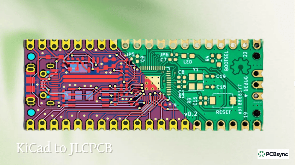
Some manufacturers now accept KiCad board files directly. JLCPCB, PCBWay, and others can process .kicad_pcb files without Gerber conversion. This simplifies the ordering process and reduces the chance of export errors.
After receiving boards, perform a visual inspection before powering anything. Check for obvious manufacturing defects, verify component orientation, and confirm solder joint quality under magnification.
Practical Tips from Years of KiCad Use
After using KiCad on dozens of projects, here are the workflow tips I wish someone had told me earlier.
Project Organization
Create a consistent folder structure for every project. I use:
Don’t modify the official libraries. Instead, create project-specific or personal libraries for components you customize or create. This prevents update conflicts and makes your projects more portable.
Keyboard Shortcuts Worth Learning
Shortcut
Action
A
Add symbol/footprint
W
Wire (schematic) / Route track (PCB)
E
Edit properties
R
Rotate
F
Flip (PCB)
X
Route differential pair
U
Select connected traces
B
Fill all zones
I
Inspect clearances
Design Rule Setup
Before starting layout, configure your design rules to match your manufacturer’s capabilities. Most PCB fabs provide design rule files or at least documented specifications. JLCPCB, PCBWay, and OSH Park all publish their capabilities, which typically include:
KiCad 9’s jobsets make this easier, but the basic process involves:
Run DRC and fix any errors
Plot Gerber files (File → Plot)
Generate drill files (Generate Drill Files button in Plot dialog)
Create pick-and-place files for assembly
Export BOM for component ordering
Most manufacturers accept KiCad’s native board files directly, but Gerbers remain the universal standard.
Common KiCad Mistakes and How to Avoid Them
Forgetting Footprint Assignments
KiCad symbols don’t automatically include footprints. After placing components in your schematic, you must assign footprints before transferring to PCB layout. Use the Footprint Assignment Tool (Tools → Assign Footprints) to handle this systematically.
Ignoring the Electrical Rules Check
ERC catches issues like unconnected pins, conflicting outputs, and missing power flags. Run ERC before starting layout and address every warning. The “power input pin not driven” error typically means you need to add a PWR_FLAG symbol to your power nets.
Skipping Design Rule Validation
Your manufacturer has limitations. If you design with 3-mil traces but your fab can only do 6-mil, you’ll have problems. Set up DRC rules before routing and let the tool catch violations as you work.
Not Using Net Classes
Assigning net classes lets you apply different design rules to different signals. Your 3.3V logic signals don’t need the same clearances as your 48V power rails. Define net classes in Schematic Setup and assign appropriate rules in Board Setup.
Troubleshooting Common KiCad Issues
Every PCB designer encounters problems. Here are solutions to issues I see repeatedly.
“Symbol not found” Errors
This usually means the library containing the symbol isn’t in your library path. Check Preferences → Manage Symbol Libraries and verify the library is listed. If you’re opening someone else’s project, they may have used custom libraries you don’t have.
Footprint Association Problems
If footprints don’t appear after transferring to PCB, the footprint library path may be incorrect. Check Preferences → Manage Footprint Libraries. Also verify that your symbol’s footprint field contains a valid library:footprint reference.
3D Models Not Displaying
3D models require correct path configuration. Check that 3D model paths in your footprints are valid and that the files exist. The KICAD7_3DMODEL_DIR environment variable should point to your 3D model collection.
DRC Reports Issues That Aren’t Real Problems
Sometimes DRC flags valid design choices as errors. You can exclude specific violations using the DRC dialog, or adjust your rules to account for intentional variations. However, be cautious about ignoring DRC errors—they often indicate real issues.
Gerber Files Look Wrong
If your exported Gerbers don’t match what you see in KiCad, check your plot settings. Verify that all layers are included, that the coordinate format matches your manufacturer’s requirements, and that the units are correct.
PCB Manufacturer Compatibility
KiCad works smoothly with virtually all PCB manufacturers. Here’s guidance for popular services.
JLCPCB
JLCPCB accepts KiCad board files directly through their website. Simply upload your .kicad_pcb file and their system processes it automatically. For assembly services, export pick-and-place files in their specified format and ensure your BOM matches their component database.
PCBWay
PCBWay accepts both Gerber files and native KiCad files. Their online Gerber viewer lets you verify your design before ordering. For prototype quantities, their pricing is competitive with other Asian manufacturers.
OSH Park
OSH Park specializes in high-quality prototype boards with their distinctive purple soldermask. They accept KiCad board files directly—just drag and drop onto their website. Pricing is per square inch, making them economical for small boards.
Eurocircuit and European Manufacturers
European manufacturers generally prefer standard Gerber formats. KiCad’s export capabilities meet all requirements. Pay attention to drill file formats—some older systems prefer specific Excellon variants.
Design for Manufacturing Considerations
Regardless of manufacturer, following DFM guidelines improves yield and reduces cost:
Maintain minimum trace width and spacing per manufacturer specs
Keep copper away from board edges (minimum 0.25mm clearance)
Size drill holes appropriately for your via and through-hole requirements
Include clear silkscreen markings for assembly orientation
Provide adequate pad-to-hole ratios for reliable soldering
Frequently Asked Questions
Is KiCad really free for commercial use?
Yes. KiCad is licensed under GPL v3, which explicitly permits commercial use. You can design products, sell boards, and run a business using KiCad without paying any licensing fees. The library components use CC-BY-SA 4.0 with an exception that allows commercial use without attribution requirements for your designs.
Can KiCad handle complex, multi-layer PCB designs?
KiCad supports up to 32 copper layers and an additional 32 technical layers. The software includes differential pair routing, length tuning, and custom design rules needed for high-speed designs. Many users successfully design DDR interfaces, USB 3.0 circuits, and other demanding applications in KiCad.
How does KiCad compare to Altium Designer?
KiCad offers most features needed for professional PCB design at no cost. Altium provides a more polished interface, better real-time collaboration tools, deeper supply chain integration, and more advanced simulation capabilities. For most individual designers and small teams, KiCad’s capabilities are sufficient. Large organizations with complex collaboration needs or regulatory requirements may benefit from Altium’s premium features.
What file formats can KiCad import and export?
KiCad imports schematics and boards from EAGLE, Altium, and several other EDA tools. It exports standard manufacturing formats including Gerber (RS-274X), Excellon drill files, IPC-2581, ODB++ (new in version 9), and various BOM formats. For mechanical integration, KiCad exports STEP and VRML 3D models.
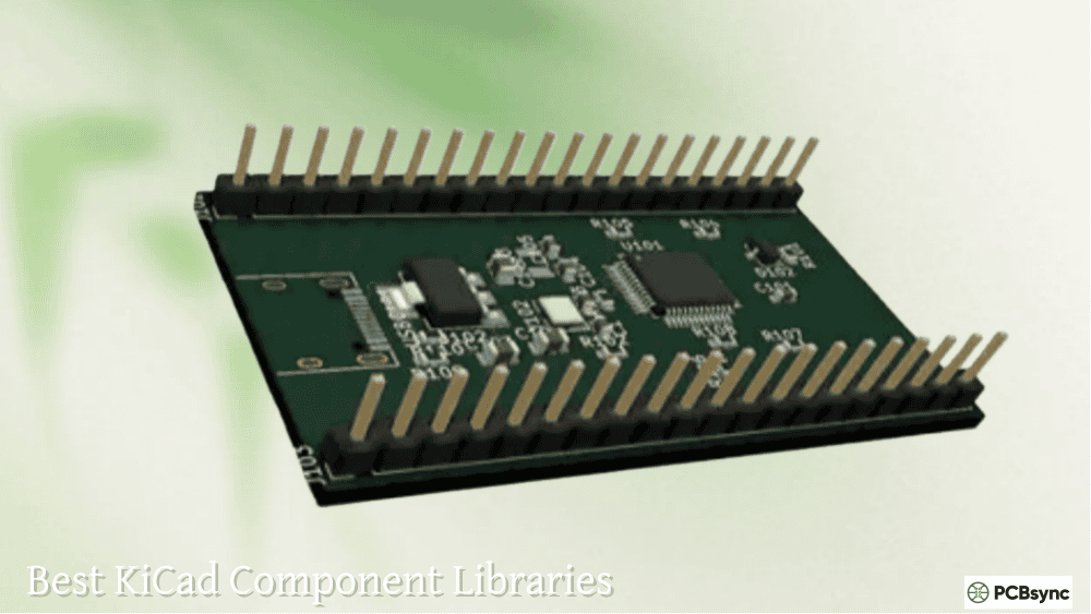
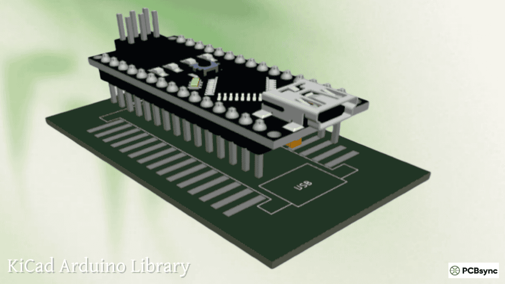
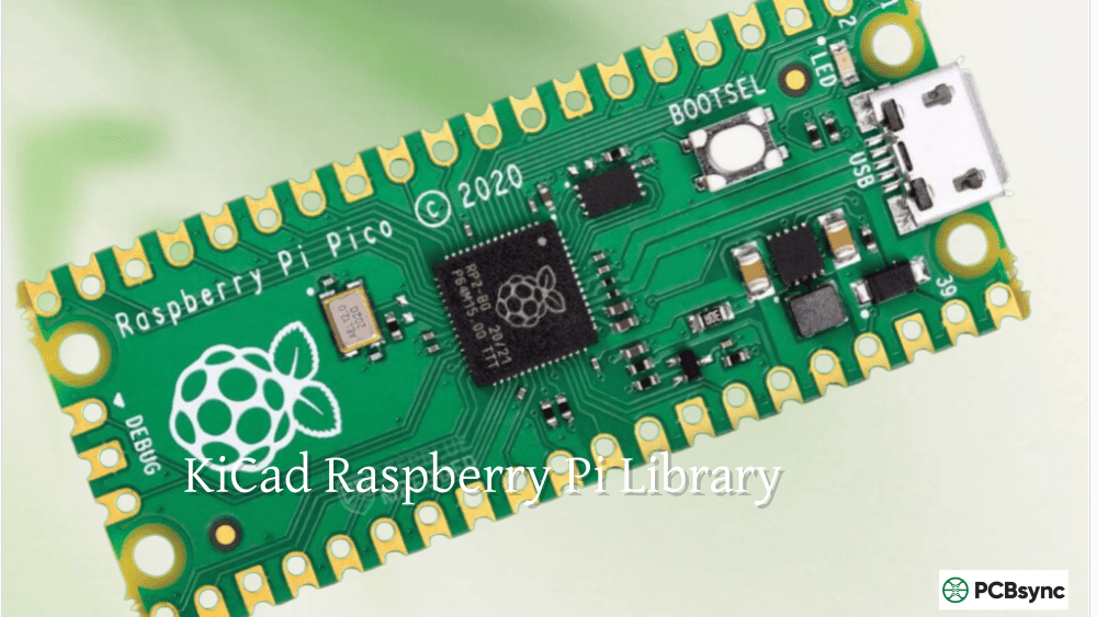
Where can I find KiCad component libraries?
KiCad includes extensive official libraries with thousands of symbols, footprints, and 3D models. Additional components are available from SnapMagic (formerly SnapEDA), Digi-Key’s KiCad library, Ultra Librarian, and the Component Search Engine. Most component sources offer free downloads in KiCad format.
Final Thoughts
KiCad has matured into a genuinely capable PCB design tool that handles professional requirements without the substantial costs of commercial alternatives. The 2026 landscape sees KiCad competing effectively against established players, backed by a dedicated development team and supportive community.
Migrating to KiCad from Other Tools
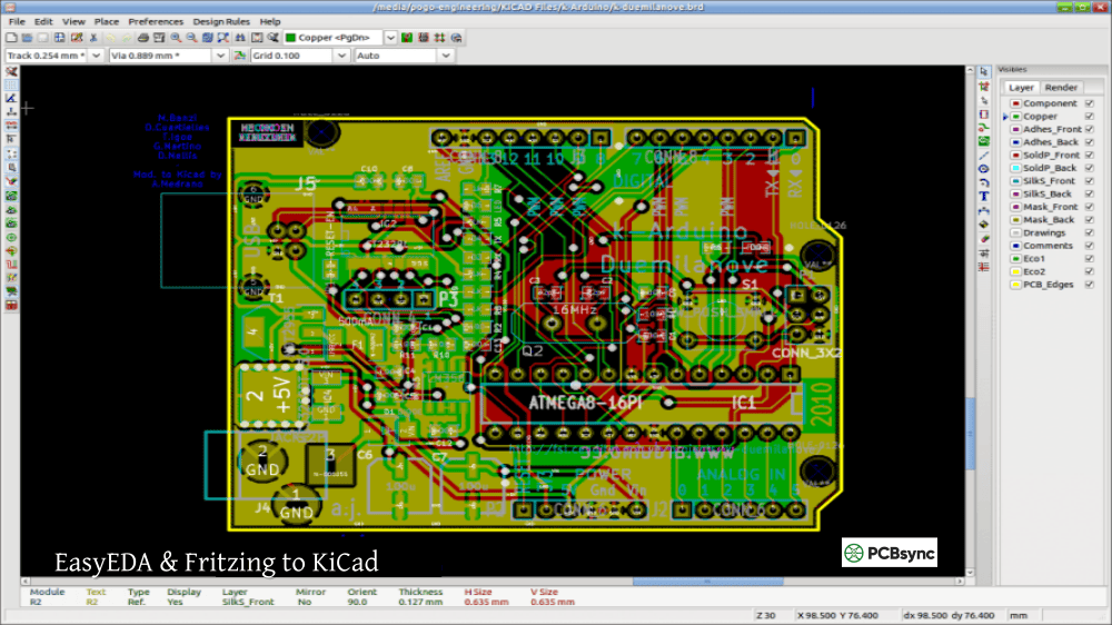
If you’re coming from another PCB design tool, KiCad provides import capabilities to ease the transition.
From EAGLE: KiCad imports EAGLE schematic (.sch) and board (.brd) files directly. The conversion handles most designs well, though you may need to manually fix some footprint assignments and verify that all components transferred correctly.
From Altium: KiCad can import Altium Designer projects, converting schematics and PCB layouts. Complex designs may require some cleanup, particularly around custom footprints and 3D models.
From OrCAD: While direct import isn’t available, you can use intermediate formats or third-party conversion tools. Many users find it easier to recreate schematics from scratch while importing the PCB layout.
Regardless of your source tool, plan for a learning curve. KiCad’s workflow differs from other tools in subtle ways. Spend time with tutorials before attempting a complex production design.
The KiCad Community
One of KiCad’s greatest strengths is its active community. The official forum at forum.kicad.info hosts thousands of discussions covering everything from basic questions to advanced techniques. Search before posting—most common questions have been answered multiple times.
The KiCad developer team actively engages with users, and feature requests submitted through proper channels often make it into future releases. The open-source nature means anyone can contribute, whether through code, documentation, library components, or translations.
Annual conferences like KiCon bring together users and developers for presentations, workshops, and networking. If you’re serious about KiCad, attending a conference accelerates your learning and connects you with the broader community.
Supporting KiCad Development
If KiCad saves you money compared to commercial alternatives, consider giving back. The Linux Foundation accepts donations on behalf of the KiCad project, funding developer time and infrastructure costs. Even small contributions help ensure continued development.
You can also contribute directly by:
Reporting bugs through GitLab
Improving documentation
Contributing to official libraries
Helping other users on the forum
Translating the interface into other languages
If you’re evaluating PCB design software, give KiCad an honest try. Download it from the official KiCad website, work through the getting started tutorial, and design a simple board. You might be surprised how capable free software has become.
The PCB design world has changed. You no longer need to spend thousands on software to create professional-quality boards. KiCad proves that open-source development can deliver tools that meet real-world engineering needs.
Inquire: Call 0086-755-23203480, or reach out via the form below/your sales contact to discuss our design, manufacturing, and assembly capabilities.
Quote: Email your PCB files to Sales@pcbsync.com (Preferred for large files) or submit online. We will contact you promptly. Please ensure your email is correct.
Notes: For PCB fabrication, we require PCB design file in Gerber RS-274X format (most preferred), *.PCB/DDB (Protel, inform your program version) format or *.BRD (Eagle) format. For PCB assembly, we require PCB design file in above mentioned format, drilling file and BOM. Click to download BOM template To avoid file missing, please include all files into one folder and compress it into .zip or .rar format.


