Inquire: Call 0086-755-23203480, or reach out via the form below/your sales contact to discuss our design, manufacturing, and assembly capabilities.
Quote: Email your PCB files to Sales@pcbsync.com (Preferred for large files) or submit online. We will contact you promptly. Please ensure your email is correct.
Notes: For PCB fabrication, we require PCB design file in Gerber RS-274X format (most preferred), *.PCB/DDB (Protel, inform your program version) format or *.BRD (Eagle) format. For PCB assembly, we require PCB design file in above mentioned format, drilling file and BOM. Click to download BOM template To avoid file missing, please include all files into one folder and compress it into .zip or .rar format.
Getting your PCB design from Altium Designer to a fabrication house shouldn’t feel like solving a puzzle. Yet every week, engineers encounter rejected uploads, missing drill files, or assembly quotes that don’t match their expectations—all because the export process wasn’t done correctly. Knowing how to properly export Altium Designer files for manufacturers like JLCPCB and PCBWay saves time, prevents costly errors, and gets your boards into production faster.
I’ve sent hundreds of designs to various PCB fabricators over the years. The export settings that work smoothly with one manufacturer might cause problems with another. This guide covers everything you need to generate manufacturer-ready files for both JLCPCB and PCBWay, including the assembly files that trip up so many engineers.
Gerber files are the universal language of PCB manufacturing. Here’s how to generate them correctly for JLCPCB and PCBWay.
Step-by-Step Gerber Export Process
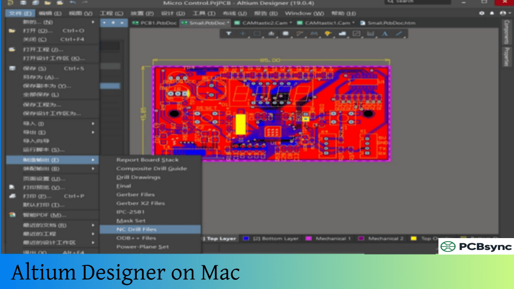
Open your PCB document in Altium Designer
Navigate to File → Fabrication Outputs → Gerber Files
The Gerber Setup dialog opens with multiple configuration tabs
General Tab Settings
Configure the basic parameters:
Units: Choose Inches or Millimeters (most manufacturers accept either)
Format: Select 2:5 for inches or 4:3 for millimeters (provides sufficient precision)
Gerber format: RS-274X (recommended) or Gerber X2 for additional embedded metadata
Layers Tab Configuration
This is where most errors occur. Select the correct layers for export:
For a standard 2-layer board, include:
Top Layer (GTL)
Bottom Layer (GBL)
Top Overlay/Silkscreen (GTO)
Bottom Overlay/Silkscreen (GBO)
Top Solder Mask (GTS)
Bottom Solder Mask (GBS)
Top Paste (GTP) – if ordering stencil or assembly
Bottom Paste (GBP) – if ordering stencil or assembly
Mechanical Layer (board outline)
Keep-Out Layer (if used for board outline)
For multilayer boards, also include:
Inner signal layers (G1, G2, G3, etc.)
Internal plane layers
Quick selection tip: Click “Plot Layers” dropdown and select “Used On” to automatically include all layers containing design data. Then verify the selection manually.
Mirror Layers Setting
Set Mirror Layers to “All Off” unless you have a specific reason to mirror (rare for standard manufacturing).
Apertures Tab
Leave the default “Embedded apertures (RS274X)” selected. This embeds aperture definitions in the Gerber files, which all modern manufacturers support.
Click OK to Generate
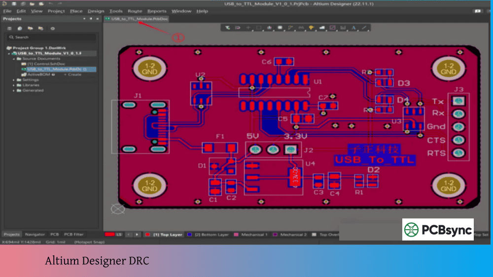
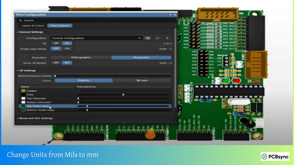
After clicking OK, Altium generates the Gerber files and automatically loads them into the CAMtastic viewer. Take a moment to scroll through each layer and verify everything looks correct before proceeding.
Generating NC Drill Files in Altium Designer
Drill files tell the manufacturer where to put holes and what sizes to use. Missing or incorrect drill files are a common cause of manufacturing delays.
Step-by-Step NC Drill Export
With your PCB open, go to File → Fabrication Outputs → NC Drill Files
The NC Drill Setup dialog appears
NC Drill Configuration Settings
Setting
Recommended Value
Notes
Units
Match Gerber settings
Use same units as Gerber for consistency
Format
2:5 (inches) or 4:3 (mm)
Match Gerber format
Zero Suppression
Suppress leading zeros
Most common format
Coordinate Positions
Reference to relative origin
Standard setting
Separate files for plated/non-plated
Enable if you have both
Creates separate drill files
Drill Drawing and Drill Guide
Consider generating drill drawing and drill guide files as well. These provide visual references that help manufacturers verify drill data. Access these through File → Fabrication Outputs → NC Drill Files and check the appropriate options.
Click OK to Generate
The drill files appear in your project folder alongside the Gerber files. For boards with multiple drill types (through-holes, blind vias, buried vias), Altium generates separate files for each drill pair.
Creating the Complete Fabrication Package
Both JLCPCB and PCBWay expect all fabrication files in a single ZIP or RAR archive.
Collecting Files for Upload
Navigate to your project output folder (usually “Project Outputs for [ProjectName]”) and verify you have:
Both JLCPCB and PCBWay offer assembly services. This requires additional files beyond the fabrication package.
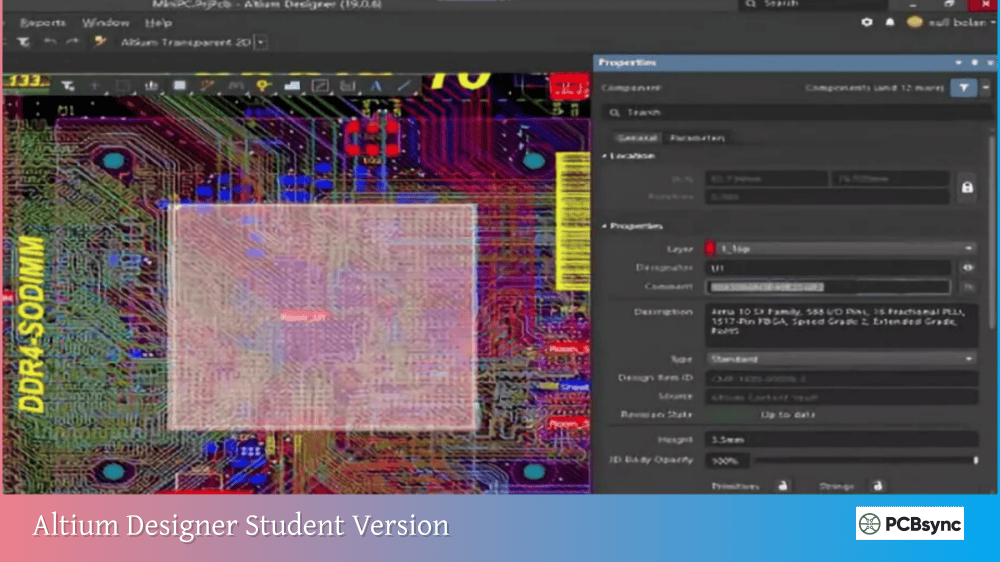
Generating the Bill of Materials (BOM)
The BOM tells the manufacturer which components go on your board.
Method 1: Direct Export from PCB Editor
Open your PCB document
Go to Reports → Bill of Materials
Configure the columns to include:
Designator
Comment (component value)
Footprint
Quantity
Manufacturer Part Number (if available)
LCSC Part Number (for JLCPCB) or supplier part number
Click Export and save as CSV or Excel format
Method 2: Using Output Job File
Add an Output Job file to your project if you don’t have one
Right-click in the “Report Outputs” section
Select Add New Report → Bill of Materials
Configure the report columns
Generate the output
BOM Format Requirements
Manufacturer
Required Columns
Part Number Column
JLCPCB
Designator, Comment, Footprint
LCSC Part Number
PCBWay
Designator, Value, Package
MPN or Supplier PN
Pro tip for JLCPCB: Add LCSC part numbers to your schematic components as a parameter. When you export the BOM, include this column to streamline the assembly quote process.
Generating Pick and Place (Centroid) Files
The pick and place file tells SMT machines exactly where to place each component.
Export Process:
Open your PCB document
Go to File → Assembly Outputs → Generate Pick and Place Files
Configure the Pick and Place Setup dialog:
Setting
Recommended Value
Units
Metric (millimeters)
Format
CSV
Include
All components or SMD only
Columns
Designator, Mid X, Mid Y, Rotation, Layer
Click OK to generate
Pick and Place File Requirements
Both JLCPCB and PCBWay require these columns:
Column
Description
Example
Designator
Component reference
C1, R5, U3
Mid X
X coordinate of component center
25.400
Mid Y
Y coordinate of component center
12.700
Rotation
Component angle in degrees
90
Layer
Top or Bottom
Top
Important: Verify that X/Y coordinates are in millimeters. Most assembly services expect metric units regardless of what you used for design.
Manufacturer-Specific Considerations
While both JLCPCB and PCBWay accept standard Gerber and Excellon files, some nuances can make your order process smoother.
JLCPCB-Specific Tips
Design Rule Files: JLCPCB provides downloadable DRC rule files (.RUL) specifically configured for their manufacturing capabilities. Import these into Altium before generating outputs:
Download the RUL file from JLCPCB’s help center
In Altium, go to Design → Rules
Right-click and select Import Rules
Run DRC with the imported rules to verify compatibility
Stackup Files: For multilayer boards, JLCPCB provides stackup files for 4-layer and 6-layer configurations. These ensure your layer assignments match their standard stackups.
LCSC Part Numbers: JLCPCB uses LCSC (their partner component distributor) for assembly. Including LCSC part numbers in your BOM significantly speeds up quoting and reduces component matching errors.
PCBWay-Specific Tips
Gerber Viewer Verification: After uploading to PCBWay, always use their online Gerber viewer to verify layer recognition. Check that:
Frequently Asked Questions About Exporting Altium Files
What Gerber format should I use—RS-274X or Gerber X2?
RS-274X works with virtually all PCB manufacturers and is the safest choice for maximum compatibility. Gerber X2 adds embedded layer metadata that can reduce miscommunication but isn’t universally supported by older CAM systems. Both JLCPCB and PCBWay accept either format. When in doubt, use RS-274X.
Why did the manufacturer detect the wrong number of layers?
This typically happens when you export layers that shouldn’t be included (empty layers, unused mechanical layers) or miss layers that should be included. Before zipping your files, open each Gerber in CAMtastic and verify it contains actual design data. Also ensure your board outline is on a mechanical layer that you’ve included in the export.
Do I need separate drill files for plated and non-plated holes?
Yes, if your design contains both plated (vias, component holes) and non-plated (mounting holes) holes. Enable the “Generate separate NC drill files for plated and non-plated holes” option in the NC Drill Setup dialog. Most manufacturers can handle combined files, but separate files eliminate any ambiguity.
How do I add LCSC part numbers to my Altium components?
Open your schematic library, select the component, and add a new parameter called “LCSC” or “LCSC Part Number” with the corresponding LCSC catalog number as the value. When you generate your BOM, include this parameter as a column. This dramatically speeds up the JLCPCB assembly quote process.
Can I send my .PcbDoc file directly to the manufacturer instead of Gerbers?
Some manufacturers accept native design files, but this isn’t recommended. Gerber files are the industry standard and give you full control over exactly what the manufacturer sees. Sending source files can lead to version compatibility issues, unintended layer exports, or exposure of proprietary design details.
Final Recommendations for Successful Exports
After years of sending designs to various manufacturers, here’s my practical advice for reliably exporting Altium Designer files:
Create a checklist: Document your export settings and verify each step. Manufacturing delays from missing files cost more than the few minutes spent double-checking.
Use Output Job files: For any design you’ll manufacture more than once, configure an Output Job. It ensures consistent outputs and prevents “I forgot to include that layer” mistakes.
Verify before uploading: Always use the manufacturer’s Gerber viewer to confirm correct layer detection, dimensions, and drill data before completing your order.
Keep outputs organized: Create a dedicated folder structure for manufacturing outputs. Include version numbers in folder names so you can trace exactly which files went to production.
Save your configuration: Once you have export settings that work for a specific manufacturer, save them. Altium allows saving Gerber and drill configurations for reuse.
The export process becomes second nature after a few successful orders. Take the time to understand what each file contains and why the manufacturer needs it. That knowledge serves you well throughout your PCB design career, regardless of which fabrication house you choose.
Inquire: Call 0086-755-23203480, or reach out via the form below/your sales contact to discuss our design, manufacturing, and assembly capabilities.
Quote: Email your PCB files to Sales@pcbsync.com (Preferred for large files) or submit online. We will contact you promptly. Please ensure your email is correct.
Notes: For PCB fabrication, we require PCB design file in Gerber RS-274X format (most preferred), *.PCB/DDB (Protel, inform your program version) format or *.BRD (Eagle) format. For PCB assembly, we require PCB design file in above mentioned format, drilling file and BOM. Click to download BOM template To avoid file missing, please include all files into one folder and compress it into .zip or .rar format.


