Inquire: Call 0086-755-23203480, or reach out via the form below/your sales contact to discuss our design, manufacturing, and assembly capabilities.
Quote: Email your PCB files to Sales@pcbsync.com (Preferred for large files) or submit online. We will contact you promptly. Please ensure your email is correct.
Notes: For PCB fabrication, we require PCB design file in Gerber RS-274X format (most preferred), *.PCB/DDB (Protel, inform your program version) format or *.BRD (Eagle) format. For PCB assembly, we require PCB design file in above mentioned format, drilling file and BOM. Click to download BOM template To avoid file missing, please include all files into one folder and compress it into .zip or .rar format.
When I started learning Altium Designer PCB design about eight years ago, the interface felt overwhelming. Panels everywhere, menu options I didn’t understand, and terminology that seemed designed to confuse newcomers. Looking back, I wish I’d had a straightforward guide that walked through the entire process from creating a project to generating manufacturing files.
This guide covers exactly that. Whether you’re transitioning from another EDA tool or starting from scratch, I’ll walk you through the complete Altium Designer PCB design workflow, from your first project to sending files to your manufacturer.
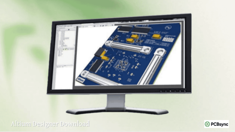
Altium Designer is a professional PCB design software package that integrates schematic capture, PCB layout, and manufacturing output generation into a single unified environment. Developed by Altium Limited, it’s used across industries from consumer electronics to aerospace and medical devices.
Unlike some tools that require separate programs for different tasks, Altium Designer handles everything in one application. Your schematic symbols link directly to PCB footprints, design rule violations appear in real-time, and manufacturing files generate from the same project file you’ve been working in throughout.
Understanding the Altium Designer PCB Design Workflow
Every Altium Designer PCB design project follows a consistent workflow. Understanding this flow before diving into the software helps you know where you’re headed at each step.
This workflow isn’t rigid. You’ll move back and forth between steps as you refine your design. Finding a component placement issue during routing? Go back and adjust. Discovering a missing connection during DRC? Return to the schematic. The key is understanding what each step accomplishes.
Setting Up Your First Altium Designer Project
Before placing any components, you need a properly configured project. This foundation determines how your schematic and PCB documents relate to each other and where your files get saved.
Creating a New PCB Project
Open Altium Designer and navigate to File > New > Project > PCB Project. This creates a project file (.PrjPcb) that acts as a container for all your design documents.
Give your project a meaningful name, as this name will appear throughout your design process and in generated files. Choose a location where you want to store all project files, keeping related documents together makes backup and version control much simpler.
Adding Design Documents
With your project created, you need to add the actual design documents:
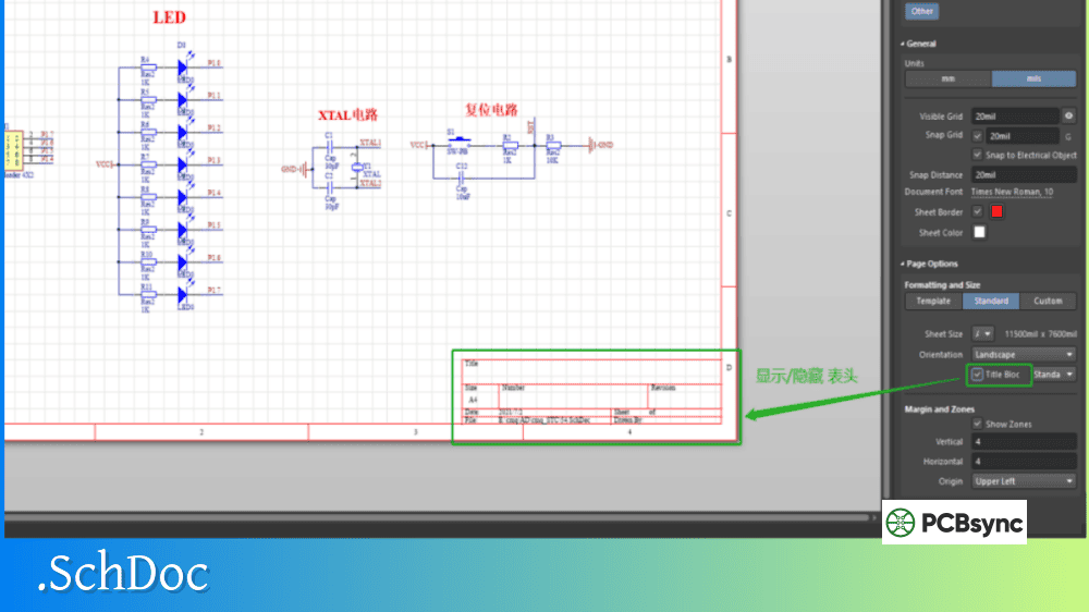
Add a Schematic Sheet: Right-click the project in the Projects panel and select Add New to Project > Schematic. This creates a .SchDoc file where you’ll capture your circuit design.
Add a PCB Document: Right-click the project again and select Add New to Project > PCB. This creates a .PcbDoc file where your physical board layout will be created.
Save both documents with descriptive names. For a single-board project, naming them the same as your project keeps things organized.
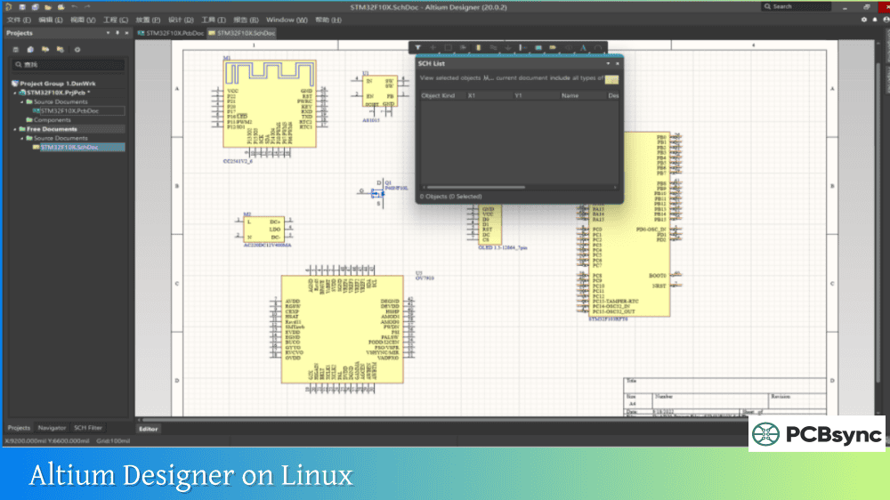
Schematic Capture in Altium Designer
Schematic capture is where you define what your circuit does electrically. Every component, every connection, and every net name you create here will transfer to your PCB layout.
Placing Components
Components come from libraries. Altium Designer includes extensive built-in libraries, and you can access millions more through the Manufacturer Part Search panel.
To place a component:
Open the Components panel (View > Panels > Components)
Search for your part by name, value, or manufacturer part number
Click the component and place it on your schematic sheet
Press Spacebar to rotate before placing if needed
When searching for components, I recommend using actual manufacturer part numbers rather than generic descriptions. Searching for “LM7805” gives you the specific regulator you want, while searching for “voltage regulator” returns thousands of options.
Wiring and Net Names
After placing components, connect them using wires (Place > Wire or shortcut P, W). Click on a pin to start a wire, click again to place a corner, and click on the destination pin to complete the connection.
For complex designs, use net labels instead of drawing wires across the entire sheet. Net labels identify connections by name. Place a net label on a pin (Place > Net Label), give it a name like “VCC” or “SPI_CLK,” and any other net label with the same name is electrically connected.
Running Electrical Rule Check (ERC)
Before moving to PCB layout, validate your schematic with the Electrical Rule Check. Navigate to Project > Compile PCB Project to run the ERC.
The Messages panel displays any violations found. Common issues include unconnected pins (floating inputs), multiple output pins connected together, and missing power connections. Address all errors and warnings before proceeding.
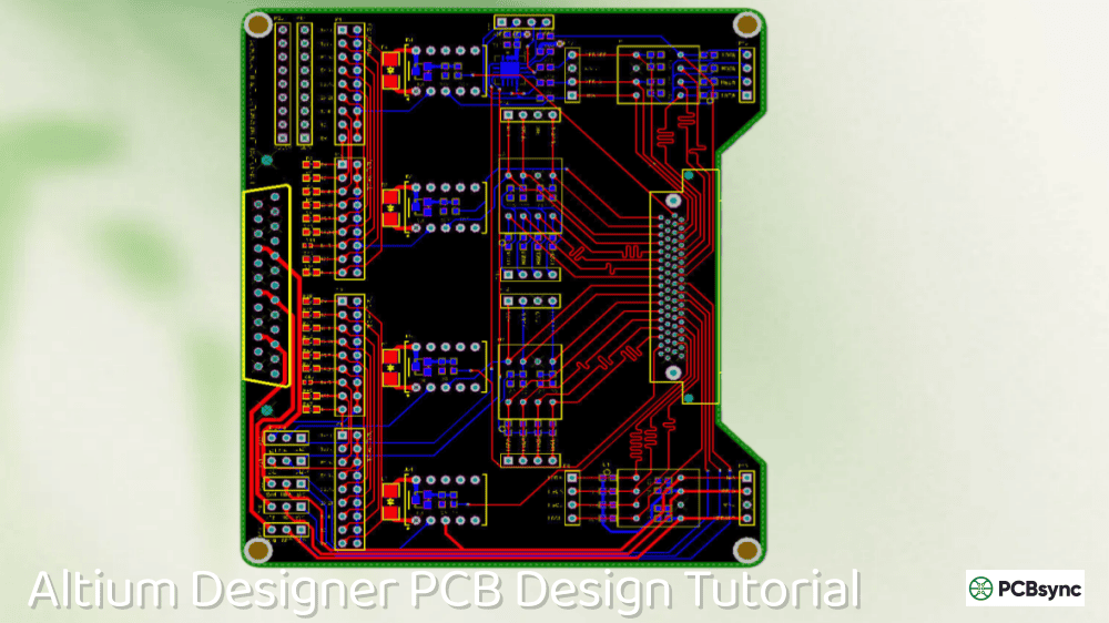
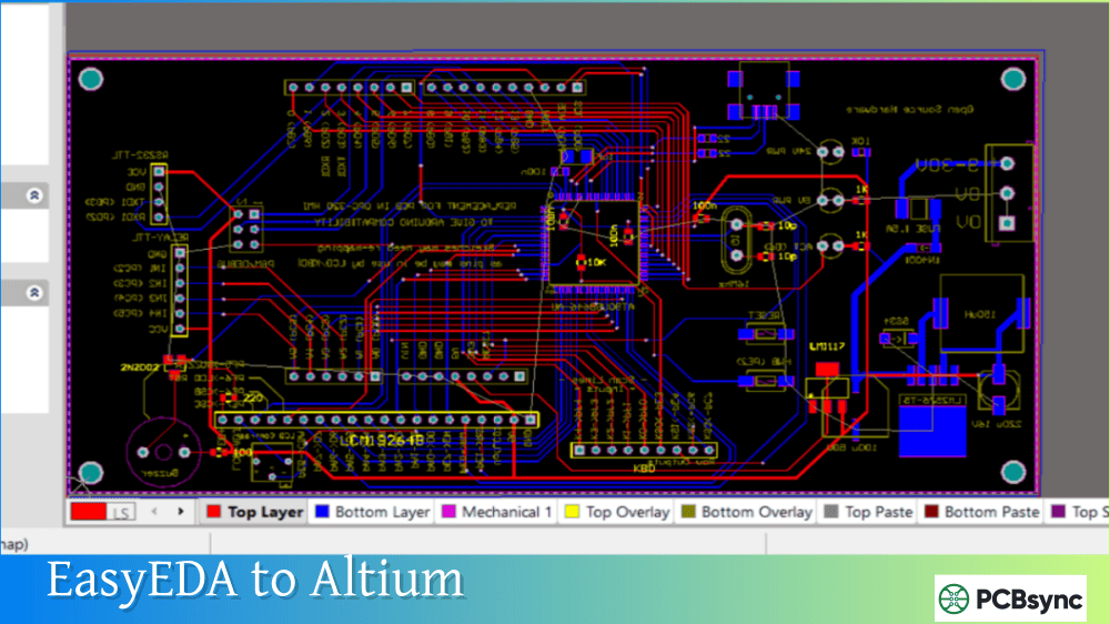
Creating Your PCB Layout
With a compiled, error-free schematic, you’re ready to create the physical PCB layout. This is where Altium Designer PCB design gets hands-on.
Defining the Board Shape
Your PCB document starts as a blank canvas. Before placing components, define your board’s physical outline:
Switch to the Keep-Out layer (press L to access the layer selector)
Use Place > Line to draw your board outline
Select Design > Board Shape > Define from Selected Objects
Confirm the board shape creation
For rectangular boards, you can also use Design > Board Shape > Redefine Board Shape and click the corners of your desired outline.
Setting Up the Layer Stackup
The layer stackup defines how many copper layers your board has and the dielectric materials between them. Access it through Design > Layer Stack Manager.
Layer Count
Typical Use
Cost Level
2 layers
Simple circuits, hobbyist projects
Low
4 layers
Most production designs, moderate complexity
Medium
6 layers
High-speed digital, dense routing
Higher
8+ layers
Complex systems, extreme density
Highest
For beginners, start with 2-layer boards. This gives you a top and bottom copper layer, which handles most simple to moderate designs. The Layer Stack Manager lets you add signal layers, plane layers (for power and ground), and configure the material properties.
Configuring Design Rules
Design rules tell Altium Designer what’s allowed in your layout. They control trace widths, clearances, via sizes, and dozens of other parameters. Access them through Design > Rules.
These values work for standard PCB manufacturing. Check with your fabricator for their specific capabilities, as advanced processes may support smaller features.
Importing Design Data from Schematic
Transfer your schematic information to the PCB using Design > Import Changes From [Project Name]. This opens the Engineering Change Order (ECO) dialog showing all changes to be made.
Click Validate Changes to verify everything can be imported, then Execute Changes to perform the import. Your components appear stacked at the origin of your PCB document, ready for placement.
Component Placement Strategies
Good component placement is half the battle in PCB design. Poor placement leads to difficult routing, signal integrity problems, and manufacturing challenges.
General Placement Guidelines
Start with constrained components: Connectors must be at board edges. Mounting holes have fixed positions. LEDs and buttons go where users can access them. Place these first before optimizing other component positions.
Group related components: Keep bypass capacitors close to their associated ICs. Place input and output stages at opposite ends of the board. Group functional blocks together.
Consider thermal management: Power components that generate heat need space around them and potentially thermal vias to inner layers or the opposite side of the board.
Plan for routing: As you place components, the ratsnest (white connection lines) shows required connections. Aim for short, uncrossed ratsnest lines, as this indicates efficient placement.
Placement Shortcuts
Shortcut
Action
Spacebar
Rotate component 90°
X
Flip component horizontally
Y
Flip component vertically
L
Move component to opposite layer
J, C
Jump to component by designator
M
Move component
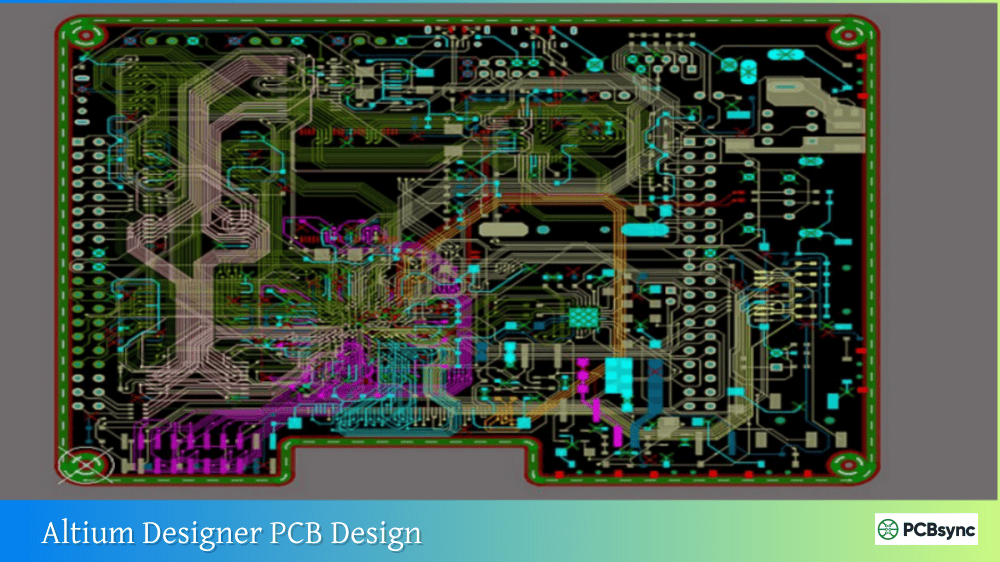
Routing Your PCB
Routing converts the logical connections from your schematic into physical copper traces on your PCB. Altium Designer offers both manual interactive routing and automatic routing options.
Interactive Routing
For most designs, interactive routing gives the best results. Start routing with Route > Interactive Routing or press P, T.
Click on a pad to start routing from that point. As you move the mouse, the trace follows with automatic obstacle avoidance. Click to place a corner, then continue to your destination. Press Spacebar to change the routing style (straight, 45°, arc) while routing.
Key Routing Shortcuts
Shortcut
Action
Spacebar
Toggle routing corner style
Shift + W
Change trace width
+ / –
Change routing layer
*
Place via and change layer
Backspace
Remove last segment
Shift + S
Toggle single layer mode
Using Polygon Pours
Ground planes improve signal integrity and simplify routing. Create them using Place > Polygon Pour:
Select the layer and net (typically GND)
Draw the polygon outline around your board area
The polygon automatically pours copper and connects to GND pads
Repour polygons after making routing changes to ensure proper copper coverage. Use Tools > Polygon Pours > Repour All to update all polygons.
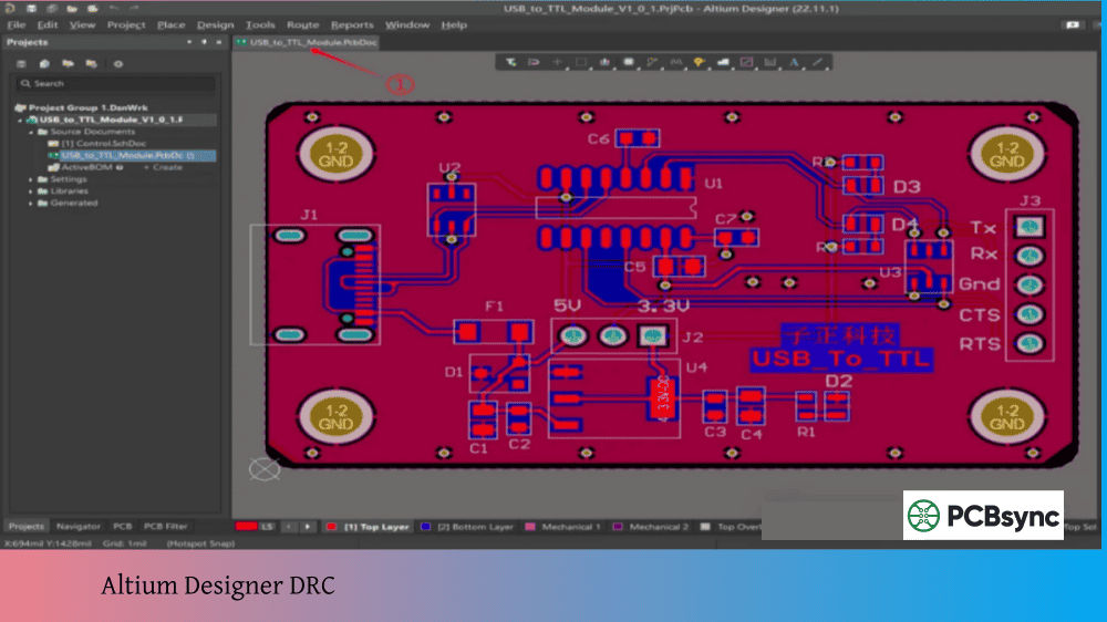
Design Rule Checking (DRC)
Before generating manufacturing files, run a comprehensive design rule check. Navigate to Tools > Design Rule Check and click Run Design Rule Check.
The DRC compares every object in your design against the rules you configured earlier. Any violations appear in the Messages panel with descriptions and the ability to zoom to the violation location.
Common DRC Violations
Violation
Cause
Solution
Clearance
Traces or pads too close together
Increase spacing or reduce trace width
Un-Routed Net
Missing connection
Complete the routing for flagged nets
Short Circuit
Unintended connection between nets
Remove the shorting trace or via
Width
Trace narrower than minimum
Increase trace width or adjust rule
Silk to Solder Mask
Silkscreen over exposed copper
Move silkscreen or adjust rule
Don’t ship a design with DRC errors. Every violation represents a potential manufacturing problem or functional failure.
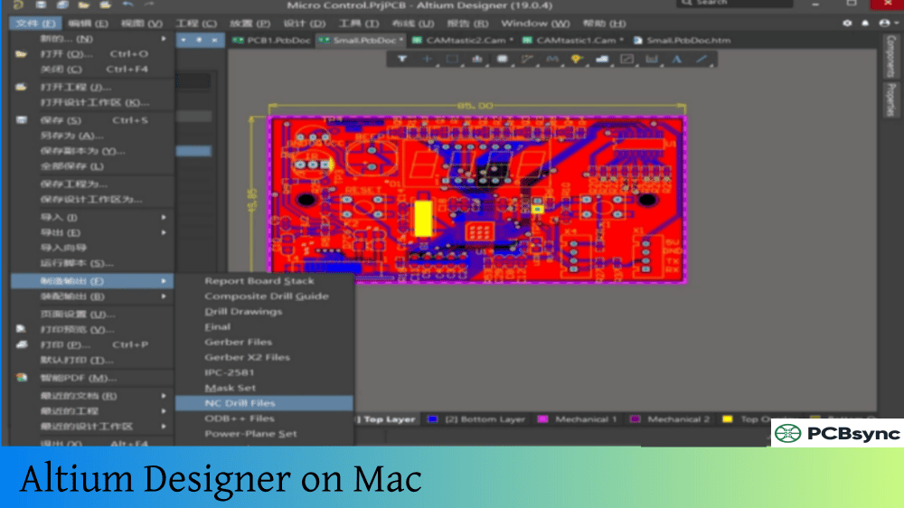
Navigate to File > Fabrication Outputs > Gerber Files. Configure the following:
General tab: Set units (millimeters or inches) and format (typically 2:5 for metric or 2:4 for imperial)
Layers tab: Select all used layers including copper, solder mask, silkscreen, and board outline
Apertures tab: Enable “Embedded apertures (RS274X)” for modern Gerber format
Click OK to generate the files. They appear in your project’s output folder.
Generating Drill Files
Navigate to File > Fabrication Outputs > NC Drill Files. Match the units and format settings to your Gerber configuration. Click OK to generate.
Creating Bill of Materials
For the BOM, use Reports > Bill of Materials or configure it in an Output Job file. Include at minimum: designator, comment/value, footprint, and manufacturer part number if available.
Frequently Asked Questions About Altium Designer PCB Design
How long does it take to learn Altium Designer PCB design?
Most engineers can complete a simple two-layer board within a week of starting with Altium Designer. Becoming proficient with the full range of features, including high-speed design rules, differential pair routing, and advanced manufacturing outputs, typically takes three to six months of regular use. The learning curve is steeper than simpler tools, but the payoff is significantly greater capability for professional designs.
What are the minimum system requirements for Altium Designer?
Altium Designer requires Windows 10 or 11 (64-bit), an Intel Core i5 or equivalent processor (i7 recommended), 8 GB RAM minimum (16 GB recommended), 10 GB of storage space, and a DirectX 11 compatible graphics card. For complex designs with large component counts or extensive 3D modeling, 32 GB RAM and a dedicated graphics card significantly improve performance.
Can I import designs from other PCB software into Altium Designer?
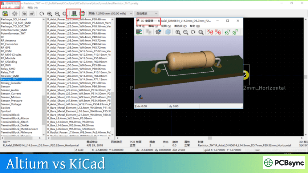
Yes, Altium Designer includes importers for most major EDA formats. You can import designs from KiCad, Eagle, OrCAD, PADS, Mentor Graphics, and other tools. The import process converts schematics, PCB layouts, and libraries, though some manual cleanup may be required depending on the source format complexity.
What’s the difference between Altium Designer and Altium 365?
Altium Designer is the desktop PCB design software you install on your computer. Altium 365 is a cloud platform that adds collaboration features, version control, and design sharing to Altium Designer. With Altium 365, multiple engineers can work on the same project, stakeholders can view designs in a web browser, and you can share manufacturing files directly with fabricators. Altium 365 requires an Altium Designer subscription.
How do I know if my PCB design is ready for manufacturing?
Your design is ready for manufacturing when it passes all design rule checks with zero errors, all nets are routed with no unconnected pins, silkscreen doesn’t overlap exposed copper, your fabricator’s design guidelines are met, and you’ve generated complete manufacturing outputs including Gerbers, drill files, and BOM. Many engineers also use Altium’s built-in Gerber viewer to visually inspect each layer before sending files to fabrication.
Moving Forward with Altium Designer PCB Design
This guide covers the fundamental workflow, but Altium Designer offers far more than we’ve touched on here. As you gain experience, explore features like hierarchical schematics for complex designs, design reuse with managed sheets, rigid-flex board design, and integration with MCAD tools for mechanical collaboration.
The best way to learn is by doing. Start with a simple project, perhaps an Arduino shield or a breakout board for a sensor. Work through the entire flow from schematic to manufacturing files. Each project builds skills that transfer to your next, more complex design.
Altium’s documentation and community resources are extensive. When you encounter something unfamiliar, the official documentation usually has the answer. For specific implementation questions, the AltiumLive forum has years of discussions covering nearly every scenario you might encounter.
This guide reflects Altium Designer features and workflow as of early 2026. The software receives regular updates that may add features or modify interfaces, so always refer to current documentation for specific version details.
Inquire: Call 0086-755-23203480, or reach out via the form below/your sales contact to discuss our design, manufacturing, and assembly capabilities.
Quote: Email your PCB files to Sales@pcbsync.com (Preferred for large files) or submit online. We will contact you promptly. Please ensure your email is correct.
Notes: For PCB fabrication, we require PCB design file in Gerber RS-274X format (most preferred), *.PCB/DDB (Protel, inform your program version) format or *.BRD (Eagle) format. For PCB assembly, we require PCB design file in above mentioned format, drilling file and BOM. Click to download BOM template To avoid file missing, please include all files into one folder and compress it into .zip or .rar format.


