Inquire: Call 0086-755-23203480, or reach out via the form below/your sales contact to discuss our design, manufacturing, and assembly capabilities.
Quote: Email your PCB files to Sales@pcbsync.com (Preferred for large files) or submit online. We will contact you promptly. Please ensure your email is correct.
Notes: For PCB fabrication, we require PCB design file in Gerber RS-274X format (most preferred), *.PCB/DDB (Protel, inform your program version) format or *.BRD (Eagle) format. For PCB assembly, we require PCB design file in above mentioned format, drilling file and BOM. Click to download BOM template To avoid file missing, please include all files into one folder and compress it into .zip or .rar format.
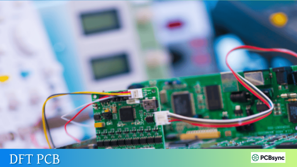
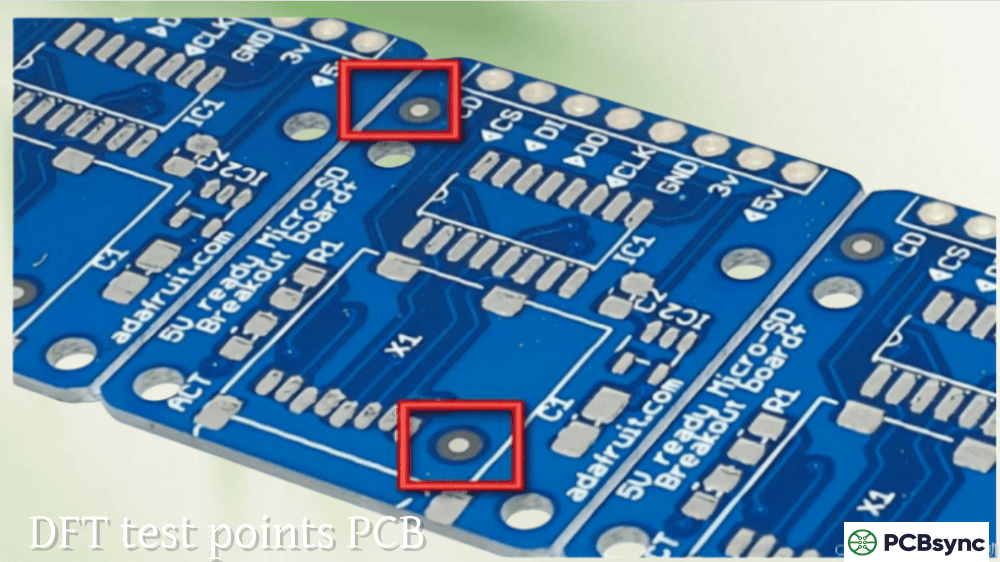
Boundary Scan Testing (JTAG) in PCB Design: A Complete DFT Guide
As PCB designs become increasingly dense with fine-pitch BGAs, multi-layer boards, and complex routing, traditional testing methods are struggling to keep up. After spending years debugging boards with inadequate test access, I can tell you that boundary scan testing has become one of the most valuable tools in my engineering toolkit. This guide covers everything you need to know about implementing JTAG-based testing in your PCB designs, from basic concepts to advanced DFT (Design for Testability) guidelines.
Boundary scan testing is a method for testing interconnections on printed circuit boards without requiring physical access to every test point. Developed by the Joint Test Action Group (JTAG) and standardized as IEEE 1149.1 in 1990, this technology embeds special test logic directly into integrated circuits.
The core idea is straightforward: instead of probing individual nets with bed-of-nails fixtures, you access test points through a dedicated serial interface built into compliant ICs. Each JTAG-compliant device contains boundary scan cells positioned between the core logic and external pins. These cells can capture input signals, drive output signals, and shift data through a chain connecting all devices on the board.
For modern boards packed with BGAs and fine-pitch components, boundary scan testing often provides the only practical way to verify that solder joints are good and signals reach their intended destinations.
How Boundary Scan Testing Works
Understanding the architecture helps you design better testable boards. Here’s what happens inside a JTAG-enabled device.
The Test Access Port (TAP)
Every IEEE 1149.1 compliant device includes a Test Access Port with four mandatory signals (plus one optional):
Signal
Function
Direction
TCK
Test Clock – synchronizes all operations
Input
TMS
Test Mode Select – controls TAP state machine
Input
TDI
Test Data In – serial data input
Input
TDO
Test Data Out – serial data output
Output
TRST
Test Reset – optional asynchronous reset
Input
The TAP controller is a 16-state finite state machine that responds to TMS sequences. It manages transitions between normal operation and various test modes, controlling which register connects between TDI and TDO at any given time.
Boundary Scan Registers and Cells
The boundary scan architecture includes several register types:
Register
Purpose
Boundary Scan Register (BSR)
Main test register containing cells at each I/O pin
Instruction Register (IR)
Holds current instruction defining test operation
BYPASS Register
1-bit register to shorten scan chain when device not under test
IDCODE Register
32-bit device identification (optional but common)
Boundary scan cells sit between each pin and the chip’s core logic. In normal operation, signals pass through transparently. During testing, these cells can be configured to capture input values, drive outputs with test patterns, or hold specific states.
Standard JTAG Instructions
IEEE 1149.1 defines mandatory and optional instructions that control boundary scan operations:
Instruction
Type
Description
EXTEST
Mandatory
Tests external interconnections between devices
SAMPLE/PRELOAD
Mandatory
Captures current pin states or preloads values for subsequent test
BYPASS
Mandatory
Bypasses device to shorten scan chain
IDCODE
Optional
Reads device identification register
INTEST
Optional
Tests internal logic using boundary scan path
HIGHZ
Optional
Places all outputs in high-impedance state
Why Boundary Scan Testing Matters for Modern PCB Design
The shift toward denser boards has fundamentally changed how we approach testing. Here’s why boundary scan testing has become essential.
BGA and Fine-Pitch Component Access
When I started working with BGA packages, the limitations of traditional ICT (In-Circuit Test) became painfully obvious. With solder balls hidden beneath the package body, there’s simply no way to physically probe these connections. Boundary scan testing provides direct access to every pin through the JTAG interface, regardless of package type.
Reduced Test Point Requirements
Traditional ICT requires a test point for every net you want to verify. On a dense 12-layer board, adding hundreds of test points consumes valuable routing space and can compromise signal integrity. Boundary scan testing lets you verify interconnections between JTAG devices with just five signals routed to a single header.
Manufacturing Fault Detection
Boundary scan testing excels at detecting common assembly defects:
Fault Type
Detection Method
Open circuits
Expected value not received at destination pin
Solder bridges/shorts
Multiple nets affected simultaneously
Missing components
No response from expected device
Wrong component
IDCODE mismatch
Stuck-at faults
Pin unable to transition between states
Component orientation errors
Incorrect pin mapping detected
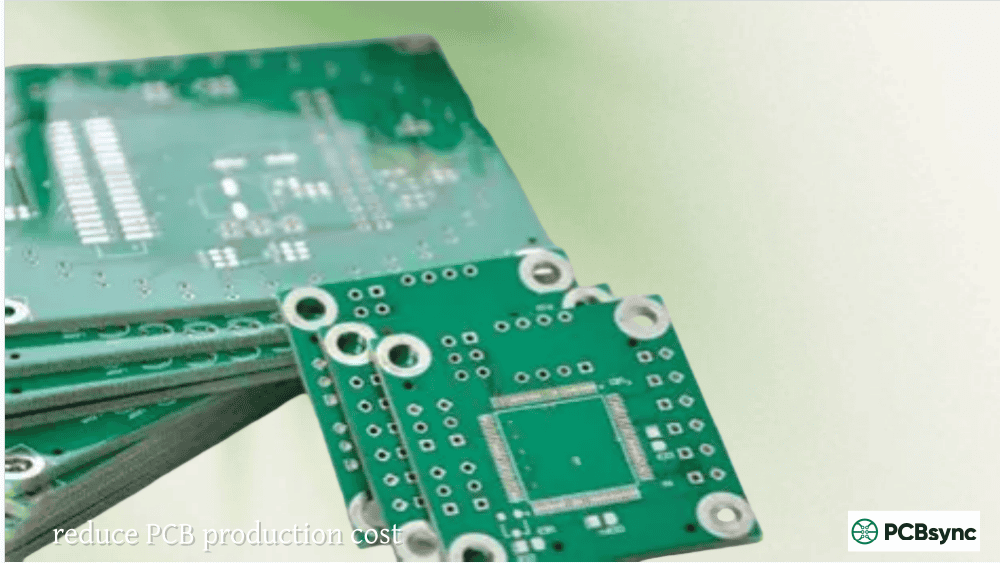
Cost Reduction
While JTAG test equipment has its own costs, the savings in fixture development and maintenance are substantial. A bed-of-nails fixture for a complex board can cost thousands of dollars and requires modification whenever the design changes. A boundary scan test connects through a simple cable to a standard header.
IEEE 1149.x Standards Family
The original IEEE 1149.1 standard has expanded into a family addressing different testing needs:
Standard
Year
Purpose
IEEE 1149.1
1990/2013
Core boundary scan standard for digital interconnects
IEEE 1149.4
1999
Mixed-signal boundary scan for analog testing
IEEE 1149.6
2003/2015
AC-coupled and differential signal testing (LVDS, etc.)
IEEE 1149.7
2009
Reduced pin count (cJTAG) for embedded systems
IEEE 1687 (iJTAG)
2014
Access to embedded instruments within devices
For high-speed designs with differential pairs and AC-coupling capacitors, IEEE 1149.6 support is particularly important. Standard 1149.1 testing can’t properly handle these signal types because it assumes DC-coupled connections.
BSDL Files: The Foundation of Boundary Scan Testing
Boundary Scan Description Language (BSDL) files are critical for implementing boundary scan testing. These files, based on a subset of VHDL, describe how the JTAG interface is implemented in each device.
What BSDL Files Contain
A BSDL file provides test software with everything needed to communicate with a device:
Section
Information Provided
Entity Description
Device name and port definitions
TAP Port Identification
Which pins are TCK, TMS, TDI, TDO, TRST
Instruction Register
Length and supported opcodes
IDCODE Register
Expected device identification value
Boundary Register
Complete description of all boundary scan cells
Package Pin Mapping
How logical ports map to physical pins
Obtaining BSDL Files
IC manufacturers are required to provide BSDL files for IEEE 1149.1 compliant devices. You can typically find them on manufacturer websites, often in the same download area as datasheets. Always verify you have the correct file for your specific device variant and package.
One thing I’ve learned the hard way: not all BSDL files are perfect. Run them through a syntax checker before relying on them for production testing. Tools like GOEPEL electronic’s free BSDL Syntax Checker can catch errors before they cause problems.
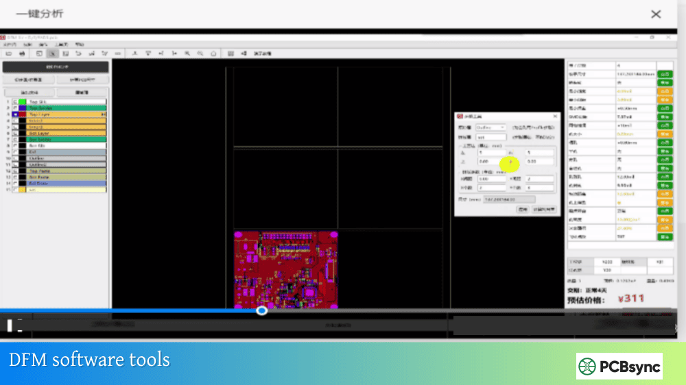
Design for Testability (DFT) Guidelines
Good boundary scan coverage doesn’t happen by accident. Following these DFT guidelines during design will maximize your test coverage and minimize debugging headaches.
Component Selection Guidelines
Choose JTAG-compliant devices whenever possible. Most modern processors, FPGAs, CPLDs, and high-pin-count devices include IEEE 1149.1 support. When selecting between similar components, the JTAG-compliant version provides significant testing advantages.
Verify BSDL file availability early. Before finalizing your BOM, confirm that valid BSDL files exist for every JTAG device. Nothing is more frustrating than discovering during test development that a critical file is missing or incorrect.
Check instruction support. At minimum, devices should support EXTEST, SAMPLE/PRELOAD, and BYPASS. Additional instructions like IDCODE and HIGHZ make testing more flexible and reliable.
Avoid dual-function JTAG pins when possible. Some devices multiplex JTAG signals with other functions. This can complicate testing if the device must be in a specific mode to enable JTAG access.
Scan Chain Design
The JTAG scan chain connects multiple devices serially, with TDO of one device feeding TDI of the next:
Keep chain length reasonable. Very long chains increase test time and can cause reliability issues. For boards with many JTAG devices, consider breaking the design into multiple chains with selective connection through a scan router device.
Route TDI/TDO correctly. TDI and TDO should form a clean daisy-chain path through all devices. Avoid stubs or branches that can cause signal integrity problems.
Connect TCK, TMS, and TRST in parallel. These signals go to all devices simultaneously. Use proper termination and consider buffering for long traces or many devices.
Never tie TRST directly to ground. This would permanently disable JTAG for the entire chain. Use a pull-down with a test header connection instead.
PCB Layout Considerations
Guideline
Rationale
Keep JTAG traces short and direct
Reduces noise and improves signal integrity
Route TAP signals away from high-speed buses
Prevents crosstalk interference
Use ground interleaving on JTAG header
Helps isolate signals during testing
Add RC termination on TCK
Reduces reflections on long traces
Provide separate TCK buffer if chain is long
Maintains signal quality
JTAG Header Design
A well-designed JTAG header makes testing reliable and convenient:
Use a standard pinout. The ARM 10-pin, 20-pin, and MIPI 10-pin formats are widely supported by test equipment. Choosing a standard pinout lets you reuse cables across projects.
Include voltage reference. Provide VTref so the test equipment knows what logic levels to use.
Key the connector. Using a keyed connector prevents insertion errors that could cause shorts between power and ground.
Maintain accessibility. Keep the JTAG header accessible even after the board is installed in an enclosure. You’ll need it for field diagnostics and firmware updates.
Pull-up and Pull-down Resistors
Proper termination prevents undefined states when the JTAG interface isn’t connected:
Signal
Recommended Pull
Value
TMS
Pull-up
4.7kΩ to 10kΩ
TCK
Pull-down
4.7kΩ to 10kΩ
TDI
Pull-up
4.7kΩ to 10kΩ
TRST
Pull-up (if used)
4.7kΩ to 10kΩ
These values provide reliable idle states without interfering with normal JTAG operation when test equipment is connected.
A typical boundary scan test development process follows these steps:
Gather inputs – Collect PCB netlist (from your EDA tool) and BSDL files for all JTAG devices
Import into test software – Load netlist and BSDL files into your boundary scan tool
Verify chain connectivity – Confirm all devices respond correctly with proper IDCODEs
Generate interconnect tests – Automated test generation for opens and shorts
Add tests for non-JTAG devices – Create patterns to test connections to non-JTAG components
Validate test coverage – Review which nets are tested and identify gaps
Debug and refine – Run tests on known-good boards and adjust as needed
Testing Non-JTAG Devices
Boundary scan testing can also verify connections to components without JTAG support, as long as those components connect to JTAG-enabled devices. By driving patterns from JTAG pins and reading responses, you can test resistor networks, LED connections, switch inputs, and simple logic devices.
For example, to test connections to a discrete buffer IC, you can drive inputs from a JTAG device’s boundary scan cells and read the outputs at another JTAG device. The buffer’s behavior (inverting or non-inverting) creates a predictable pattern that verifies connectivity.
Power supply connections – Cannot be tested through boundary scan
Non-JTAG device internals – Only connections to JTAG devices are directly testable
Test Time Optimization
Long scan chains and complex patterns can make test times impractical. Strategies for improvement include using BYPASS on devices not under test, optimizing pattern generation settings, and using parallel programming for multi-device configurations.
Frequently Asked Questions
What is the difference between JTAG and boundary scan testing?
Technically, JTAG refers to the Joint Test Action Group that developed the standard and, by extension, the test access port interface with its TDI, TDO, TCK, and TMS signals. Boundary scan testing specifically describes using that interface to test PCB interconnections through the boundary scan cells in compliant devices. In practice, people use the terms interchangeably, though JTAG also encompasses debugging and programming applications beyond boundary scan testing.
How much board coverage can boundary scan testing achieve?
Coverage depends heavily on your design. A board populated entirely with JTAG-compliant devices might achieve 95% or higher coverage of digital interconnects. Realistically, most designs include non-JTAG components that reduce this number. Typical production boards see 60-85% coverage from boundary scan testing alone. Combining boundary scan testing with functional tests or limited ICT can push total coverage above 95%.
Does boundary scan testing replace In-Circuit Testing (ICT)?
Boundary scan testing complements rather than replaces ICT. While boundary scan testing excels at interconnect verification with minimal physical access requirements, ICT can measure component values, test analog circuits, and verify power rails. Many manufacturers use both: boundary scan testing for high-density digital sections and ICT for analog and power testing. The trend is toward increasing boundary scan coverage to reduce fixture complexity.
What does it cost to implement boundary scan testing?
Costs vary widely based on your requirements. Entry-level boundary scan tools start around $5,000-10,000 for basic software with a USB JTAG adapter. Mid-range systems with better diagnostics and programming features run $15,000-40,000. High-end production systems with advanced diagnostics, multiple JTAG ports, and ICT integration can exceed $100,000. Compare these costs against fixture development ($5,000-50,000 per board design) and debugging time saved.
Can boundary scan testing detect all manufacturing defects?
No. Boundary scan testing is excellent for interconnect defects like opens, shorts, and missing devices but cannot detect all possible faults. It won’t find problems with power supply sequencing, timing-related issues, parametric failures, or defects inside non-JTAG components. A comprehensive test strategy combines boundary scan testing with other methods including functional testing, automated optical inspection, and selective ICT to achieve high defect coverage.
Conclusion
Boundary scan testing has evolved from a specialized technique into a fundamental tool for PCB testing. As component packages continue shrinking and board densities increase, the value of JTAG-based testing only grows. By following the DFT guidelines in this article, selecting appropriate components with good BSDL support, and designing clean scan chains with proper accessibility, you can achieve reliable test coverage without the expense and limitations of traditional bed-of-nails approaches.
The key is thinking about testability from the start of your design. Adding JTAG support as an afterthought rarely works well. But when boundary scan testing is planned into the architecture, it becomes a powerful tool that serves you through prototyping, production, and field service.
Start with your next design: verify BSDL availability for your key components, plan your scan chain topology, and include a properly designed JTAG header. Your future self, debugging that first prototype at midnight before a deadline, will thank you.
Inquire: Call 0086-755-23203480, or reach out via the form below/your sales contact to discuss our design, manufacturing, and assembly capabilities.
Quote: Email your PCB files to Sales@pcbsync.com (Preferred for large files) or submit online. We will contact you promptly. Please ensure your email is correct.
Notes: For PCB fabrication, we require PCB design file in Gerber RS-274X format (most preferred), *.PCB/DDB (Protel, inform your program version) format or *.BRD (Eagle) format. For PCB assembly, we require PCB design file in above mentioned format, drilling file and BOM. Click to download BOM template To avoid file missing, please include all files into one folder and compress it into .zip or .rar format.


