Inquire: Call 0086-755-23203480, or reach out via the form below/your sales contact to discuss our design, manufacturing, and assembly capabilities.
Quote: Email your PCB files to Sales@pcbsync.com (Preferred for large files) or submit online. We will contact you promptly. Please ensure your email is correct.
Notes: For PCB fabrication, we require PCB design file in Gerber RS-274X format (most preferred), *.PCB/DDB (Protel, inform your program version) format or *.BRD (Eagle) format. For PCB assembly, we require PCB design file in above mentioned format, drilling file and BOM. Click to download BOM template To avoid file missing, please include all files into one folder and compress it into .zip or .rar format.
How to Reduce PCB Production Costs with DFX Strategies
Here’s a number that should get every product manager’s attention: 75-85% of your product’s manufacturing cost is locked in during the design phase. By the time your PCB reaches production, most cost-saving opportunities have already passed. The decisions made during schematic capture and layout—component selection, layer count, board dimensions, via strategy—determine what you’ll pay for every unit produced.
After eighteen years of designing boards and watching projects blow through budgets, I’ve learned that the most effective way to reduce PCB production cost isn’t negotiating harder with suppliers or cutting corners on materials. It’s implementing Design for Excellence (DFX) strategies from the earliest design stages. When you embed cost consciousness into your design methodology, savings compound at every production step.
Understanding DFX: The Framework for Cost-Effective Design
Design for Excellence (DFX) is a comprehensive design philosophy where the “X” represents different optimization targets. While excellence is the overarching goal, each DFX discipline addresses specific aspects of the product lifecycle:
DFX Discipline
Focus Area
Cost Impact
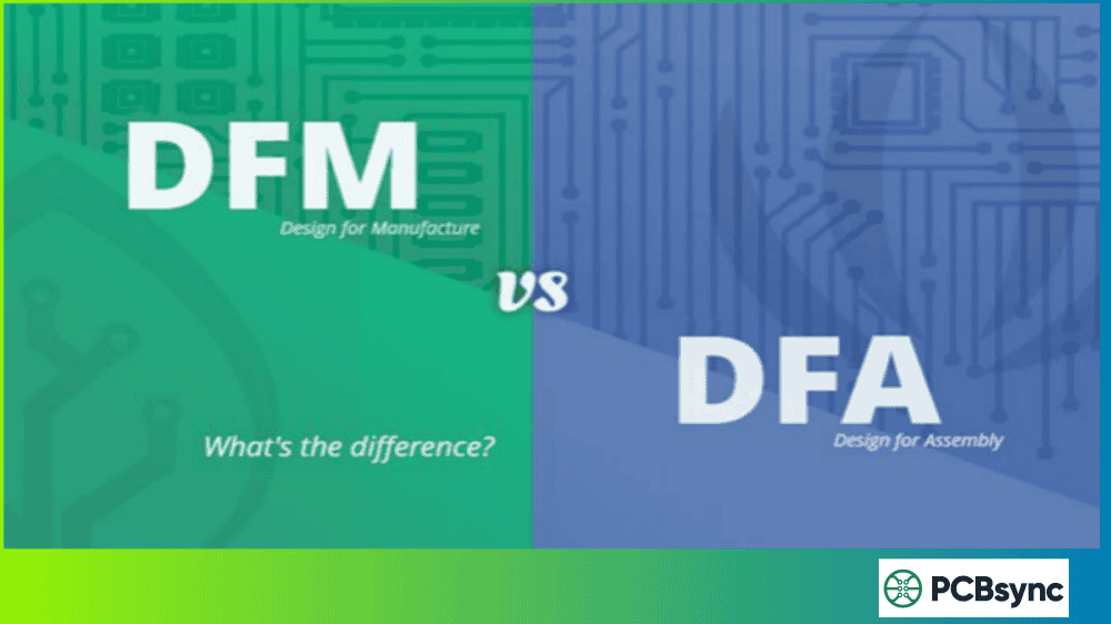
DFM (Design for Manufacturing)
Bare board fabrication
15-40% fabrication savings
DFA (Design for Assembly)
Component placement and soldering
10-25% assembly savings
DFT (Design for Testability)
Quality verification and debugging
20-50% test cost reduction
DFC (Design for Cost)
Overall product economics
10-30% total cost reduction
DFR (Design for Reliability)
Long-term performance
Reduced warranty and field failure costs
The power of DFX lies in addressing problems when solutions are cheap. A layer reduction during layout costs nothing but engineering time. The same change after production tooling might require complete redesign. Let’s explore how each DFX strategy helps reduce PCB production cost.
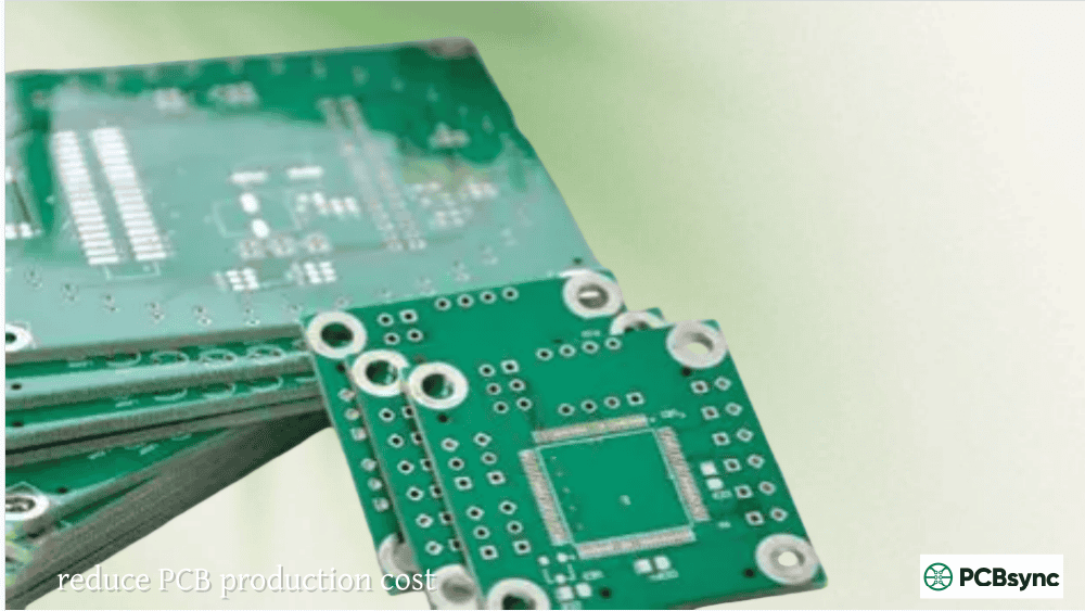
DFM Strategies to Reduce PCB Fabrication Costs
PCB fabrication typically accounts for 8-12% of total product cost, but design decisions that affect fabrication ripple through assembly, test, and field reliability. Optimizing for manufacturability creates savings across the entire production chain.
Layer Count Optimization
Layer count is one of the most significant cost drivers in PCB fabrication. Each additional layer adds lamination cycles, drilling operations, and material costs.
Layer Count
Relative Cost
Typical Applications
2-layer
1.0x (baseline)
Simple consumer products
4-layer
1.5-2.0x
Most embedded systems
6-layer
2.5-3.0x
Complex digital designs
8-layer
3.5-4.5x
High-speed, dense designs
10+ layers
5.0x+
Server, networking, aerospace
Cost Reduction Strategy: Before accepting a 6-layer design as necessary, invest time in layout optimization. Aggressive routing, strategic component placement, and careful power distribution can often reduce layer count. Dropping from 6 to 4 layers typically saves 30-40% on fabrication costs.
Via Strategy Management
Vias connect signals between layers, but different via types carry dramatically different cost implications:
Cost Reduction Strategy: Use through-hole vias whenever possible. Reserve blind, buried, and microvias for high-density designs where routing density absolutely requires them. A design using only through-hole vias is significantly cheaper to fabricate than one requiring HDI processes.
Board Size and Panelization
Your board dimensions directly affect how many pieces fit on a standard pcb manufacturing panel (typically 18″ x 24″). Poor panel utilization means you’re paying for wasted material.
Cost Reduction Strategy: When possible, design board dimensions that maximize panel utilization. A board that’s 95mm x 95mm might fit 20 pieces per panel, while a 100mm x 100mm board might only fit 16—a 20% reduction in yield from a 5% size increase. Work with your fabricator early to understand panel sizes and optimize accordingly.
Standard Specifications vs. Premium Features
Every deviation from standard manufacturing capabilities adds cost:
Cost Reduction Strategy: Design to standard specifications unless performance requirements demand otherwise. That 4-mil trace you used because it fit the routing might cost 20% more than a 5-mil trace that requires slightly different placement.
DFA Strategies to Reduce PCB Assembly Costs
Assembly often represents 15-30% of total PCBA cost. Design decisions that simplify assembly, reduce component count, and enable automation directly reduce PCB production cost.
Component Consolidation and Standardization
Every unique component in your BOM adds procurement complexity, inventory costs, and potential for assembly errors.
Cost Reduction Strategy:
Consolidate resistor and capacitor values where tolerances allow
Standardize on common package sizes across designs
Reduce the number of unique part numbers in your library
Use the same component for multiple functions when possible
A design with 50 unique part numbers costs significantly more to assemble than one with 30 unique parts, even if total component count is similar.
Single-Sided vs. Double-Sided Assembly
Assembling components on both sides of a PCB requires two placement passes and two reflow cycles, roughly doubling assembly time.
Cost Reduction Strategy: If you have only a few components on the secondary side, consider redesigning to consolidate everything on one side. The fabrication cost of a slightly larger board is often less than the assembly cost of double-sided placement.
Component Package Selection
Package size affects both component cost and assembly cost:
Package Size
Component Cost Trend
Assembly Complexity
0201
Higher
High (specialized equipment)
0402
Moderate
Moderate
0603
Lower
Low
0805
Lowest
Very low
Cost Reduction Strategy: Don’t automatically select the smallest available package. For passive components where space permits, 0603 or 0805 packages are often cheaper to procure AND cheaper to assemble than 0402 or 0201.
Orientation and Placement Consistency
Consistent component orientation simplifies pick-and-place programming and visual inspection.
Cost Reduction Strategy: Orient all polarized components consistently (all diodes cathodes pointing the same direction, all ICs with pin 1 in consistent position). This reduces programming time and assembly errors, both of which affect cost.
DFT Strategies to Reduce Test Costs
Testing can represent 5-15% of production cost, but more importantly, inadequate test access leads to escaped defects that cost far more to fix in the field.
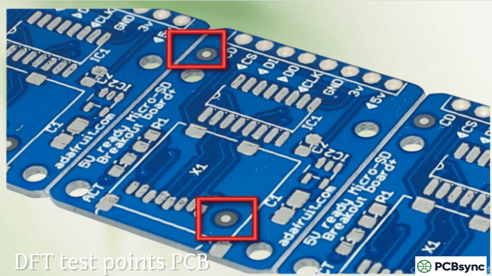
Test Point Strategy
Designing adequate test access reduces test time and enables more complete coverage:
Design test points on one side of the board when possible (reduces fixture cost)
Maintain minimum 100-mil spacing between test points for bed-of-nails fixtures
Place test points on a regular grid to simplify fixture design
A board with good test access might achieve 95%+ coverage with a simple fixture, while poor test access might require expensive flying probe testing or accept lower coverage.
Design for Debug
Boards that are difficult to debug during bring-up consume engineering time—an often-overlooked cost.
Cost Reduction Strategy: Include debug headers, test points on key signals, and clear silkscreen labeling. The small additional PCB cost is recovered many times over in reduced debug time during development and production troubleshooting.
Design for Cost takes a holistic view, considering not just fabrication and assembly but total lifecycle economics.
Component Lifecycle Management
A component going end-of-life (EOL) forces redesign—an expensive proposition that DFC methodology prevents.
Cost Reduction Strategy:
Check component lifecycle status before design commitment
Prefer components from multiple manufacturers (second sources)
Avoid components already marked “not recommended for new designs”
Consider last-time-buy quantities for long-lifecycle products
Volume Considerations
Per-unit costs decrease dramatically with volume due to amortized setup costs:
Order Volume
Relative Per-Unit Cost
10 units
5-10x
100 units
2-3x
1,000 units
1.0x (baseline)
10,000 units
0.6-0.8x
100,000+ units
0.3-0.5x
Cost Reduction Strategy: If prototyping costs seem high, remember that setup costs dominate small orders. Consider ordering slightly larger prototype quantities if you expect multiple development builds anyway.
Material Selection Economics
Material choices extend beyond the PCB substrate to affect the entire production chain:
Cost Reduction Strategy:
Use standard FR-4 unless thermal or high-frequency requirements demand otherwise
Avoid exotic materials (Rogers, ceramic, polyimide) unless performance mandates them
A wireless module might cost $40/board with Rogers material and $10/board with optimized high-Tg FR-4—a 75% savings if FR-4 meets performance requirements.
Implementing DFX in Your Design Process
Early Engagement with Manufacturing Partners
The most effective DFX happens through collaboration. Engage your CM or fabricator during design, not after Gerber release.
Implementation Steps:
Request manufacturer design rules before starting layout
Share preliminary designs for DFM/DFA review
Discuss production volumes and cost targets
Incorporate feedback before finalizing design
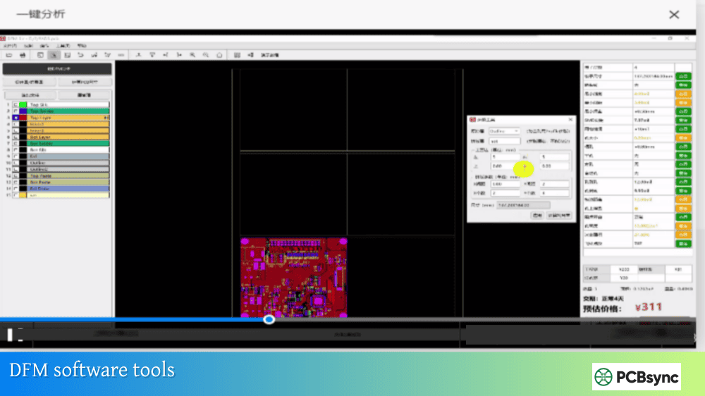
Using DFX Analysis Tools
Modern EDA tools include built-in DFX checking capabilities:
Implementation Strategy: Track estimated production cost throughout the design process. When adding features or complexity, understand the cost impact before committing. A design change that adds $0.50 per unit might be acceptable—or might destroy product margins depending on volume.
Frequently Asked Questions About Reducing PCB Production Cost
What is the single most effective way to reduce PCB production cost?
Layer count reduction typically offers the highest impact for fabrication costs—dropping from 6 to 4 layers can save 30-40% on bare board costs. However, component cost usually dominates total PCBA cost (60-70%), so BOM optimization often yields the largest absolute savings. The most effective approach combines both: optimize the design to minimize layers while standardizing and consolidating components. DFX analysis early in design identifies which opportunities apply to your specific product.
How much can DFX strategies typically save on production costs?
Comprehensive DFX implementation typically achieves 10-30% total cost reduction compared to designs developed without systematic cost optimization. Individual strategies vary: layer reduction might save 30-40% on fabrication, component consolidation might save 10-15% on procurement, and test optimization might save 20-50% on quality verification. The key is applying DFX early when design flexibility is highest. Changes made after production tooling cost 10-100 times more than changes made during initial design.
Should I use the cheapest PCB fabricator to reduce costs?
Price alone is a poor selection criterion. The cheapest fabricator might have lower yields, longer lead times, or quality issues that ultimately cost more than a slightly higher-priced but more reliable supplier. Evaluate total cost of ownership including yield rates, on-time delivery, quality consistency, and engineering support. A fabricator with robust DFM feedback might cost 5% more per board but save 20% through design optimization suggestions. Establish relationships with fabricators who offer design support and can grow with your volume requirements.
How do I balance cost reduction with product reliability?
DFX strategies should never compromise reliability—properly implemented, they often improve it. A design with fewer layers but adequate power distribution is both cheaper and more reliable than an over-designed board. The key is understanding which specifications are truly required versus which represent over-engineering. Use DFR (Design for Reliability) analysis to identify actual reliability requirements, then apply DFC (Design for Cost) to meet those requirements economically. Cost and reliability aren’t inherently opposed; poor design creates both cost and reliability problems.
When is it worth paying premium for advanced PCB features?
Premium features like HDI, blind/buried vias, or exotic materials make sense when they enable capabilities that standard technology cannot achieve, or when their cost premium is offset by other savings. For example, HDI might cost more per square inch but enable a smaller board that reduces total cost. High-frequency materials might be essential for RF performance. Evaluate premium features based on total product cost and performance requirements, not just PCB fabrication cost. Sometimes paying more for the board saves money elsewhere in the system.
Building Cost Consciousness Into Design Culture
The most successful engineering teams treat cost as a design constraint, not an afterthought. This means:
Setting Cost Targets Early: Establish target cost during product definition, before design begins. This frames every subsequent decision.
Tracking Costs Throughout Design: Monitor estimated production cost as design progresses. Understand the cost impact of each design decision.
Collaborating Across Functions: Involve manufacturing, procurement, and quality engineering in design reviews. Their perspectives identify cost reduction opportunities designers might miss.
Learning from Production: Track actual production costs against estimates. Understand where predictions were accurate and where they missed. Apply lessons to future designs.
The goal isn’t to reduce PCB production cost at any expense—it’s to build products that meet performance requirements at the lowest sustainable cost. DFX strategies make this possible by systematically addressing cost throughout the design process, when solutions are cheapest to implement.
Every board you design represents an opportunity to apply these principles. The engineers who master DFX don’t just design circuits that work—they design circuits that work economically. In competitive markets, that capability determines which products succeed and which never make it to production.
Inquire: Call 0086-755-23203480, or reach out via the form below/your sales contact to discuss our design, manufacturing, and assembly capabilities.
Quote: Email your PCB files to Sales@pcbsync.com (Preferred for large files) or submit online. We will contact you promptly. Please ensure your email is correct.
Notes: For PCB fabrication, we require PCB design file in Gerber RS-274X format (most preferred), *.PCB/DDB (Protel, inform your program version) format or *.BRD (Eagle) format. For PCB assembly, we require PCB design file in above mentioned format, drilling file and BOM. Click to download BOM template To avoid file missing, please include all files into one folder and compress it into .zip or .rar format.


