Inquire: Call 0086-755-23203480, or reach out via the form below/your sales contact to discuss our design, manufacturing, and assembly capabilities.
Quote: Email your PCB files to Sales@pcbsync.com (Preferred for large files) or submit online. We will contact you promptly. Please ensure your email is correct.
Notes: For PCB fabrication, we require PCB design file in Gerber RS-274X format (most preferred), *.PCB/DDB (Protel, inform your program version) format or *.BRD (Eagle) format. For PCB assembly, we require PCB design file in above mentioned format, drilling file and BOM. Click to download BOM template To avoid file missing, please include all files into one folder and compress it into .zip or .rar format.
Improve PCB Yield Rate: DFM & DFA Techniques That Work
Here’s a statistic that haunts production managers: the average first-pass yield for electronics manufacturers using SMT is only 80%. That means one in five boards requires rework, repair, or scrapping before it can ship. For complex assemblies, that number can drop even lower. The cost multiplier is brutal—fixing a defect after reflow costs 10 times more than catching it at solder paste printing, and 100 times more if it escapes to final test.
After seventeen years of chasing yield problems from prototype through volume production, I’ve learned that PCB yield improvement isn’t primarily about fixing manufacturing processes. It’s about preventing yield problems during design. The boards that achieve 98-99% first-pass yields aren’t lucky—they’re designed for manufacturability from the start.
Yield rate measures the percentage of boards that pass quality standards without rework or repair. First-pass yield (FPY) specifically measures boards that pass on the first attempt through any given test station.
The economics are straightforward: higher yield means lower cost per good unit. But yield impacts more than direct costs. Low-yield products create scheduling chaos, consume engineering time for troubleshooting, and strain customer relationships when deliveries slip.
First-Pass Yield
Defect Rate
Impact on 1,000 Board Run
99%
1%
10 boards need rework
95%
5%
50 boards need rework
90%
10%
100 boards need rework
80%
20%
200 boards need rework
The relationship between yield and profit is nonlinear. Moving from 90% to 95% yield eliminates 50 rework events per thousand boards. Moving from 95% to 99% eliminates only 40 more—but those last percentage points often represent the hardest defects to eliminate.
DFM Techniques for PCB Yield Improvement
Design for Manufacturing (DFM) ensures your PCB design aligns with fabrication capabilities. DFM problems create yield losses at bare board production, and those problems cascade through assembly, creating additional defects downstream.
Yield Improvement Strategy: Design to 80% of manufacturer capability, not 100%. If your fabricator can reliably produce 4-mil traces, design with 5-mil minimum. The extra margin absorbs normal process variation without creating defects.
Via Design and Placement
Vias are one of the highest-defect-density features in PCB fabrication. Improper via design creates plating voids, annular ring breakout, and registration problems.
DFM Rules for Higher Via Yield:
Maintain minimum 8-mil drill-to-copper clearance
Keep aspect ratios below 10:1 for through-holes
Use teardrops on trace-to-pad connections for marginal annular rings
Avoid via-in-pad unless you’ve confirmed your fabricator’s fill and cap process
Copper Balance and Warpage Prevention
Unbalanced copper distribution causes board warpage during fabrication and reflow. Warped boards create assembly defects—poor stencil contact, component placement errors, and reflow failures.
Yield Improvement Strategy: Balance copper weight between top and bottom layers. Fill empty areas with copper pour (tied to ground or floating, depending on signal integrity requirements). A well-balanced board stays flat through thermal cycling, improving yield at every subsequent assembly step.
Acid Traps and Sliver Prevention
Acute angles in traces create acid traps where etchant collects, potentially eating through copper and creating opens. Thin copper features (slivers) can detach during fabrication and cause shorts elsewhere on the board.
DFM Rules:
Avoid trace angles less than 90 degrees
Eliminate copper features narrower than 4 mils
Review copper pours for thin necks that could break
Use DFM analysis tools to automatically flag these issues
DFA Techniques for Assembly Yield Improvement
Design for Assembly (DFA) optimizes your design for efficient, error-free component placement and soldering. DFA problems directly cause assembly defects—tombstoning, bridging, misalignment, and solder voids.
Component Spacing and Clearances
Inadequate spacing creates multiple yield problems: pick-and-place machines can’t grip components, rework becomes impossible, and solder bridges form between adjacent pads.
Component Relationship
Minimum Clearance
Recommended
Yield Benefit
SMD to SMD
10 mils
20-30 mils
Eliminates bridging risk
SMD to THT
40 mils
60 mils
Enables wave soldering
Component to board edge
100 mils
125 mils
Prevents depanel damage
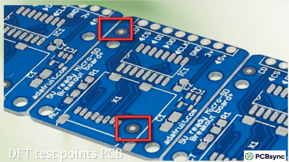
Component to test point
50 mils
100 mils
Enables ICT access
Yield Improvement Strategy: Don’t design to minimum clearances unless space constraints demand it. Every component placed at minimum spacing represents elevated yield risk.
Thermal Balance for Soldering
Tombstoning—where one end of a passive component lifts during reflow—is one of the most common assembly defects. It results from unequal heating of the two pads, causing asymmetric solder surface tension.
DFA Rules to Prevent Tombstoning:
Use identical pad sizes on both ends of passive components
Match trace widths connecting to each pad
Apply thermal reliefs to pads connected to ground planes
Orient components consistently relative to reflow direction
A surface-mount PCB that experienced 10% yield loss from solder bridges was redesigned with wider pad spacing. The change improved yield to 99%—a dramatic improvement from a simple design modification.
Footprint Accuracy and BOM Validation
Footprint-to-component mismatches cause catastrophic yield loss. If the land pattern doesn’t match the actual component, nothing the assembly line does can create reliable solder joints.
DFA Validation Checklist:
Cross-reference every footprint against manufacturer datasheet
Verify pin numbering matches component and schematic symbol
Check polarity markings on footprints for polarized components
Automated DFA tools can catch many of these mismatches, but manual review remains essential for custom or unusual components.
Solder Mask Design for Assembly Yield
Solder mask controls where solder flows during reflow. Inadequate mask design causes bridging, solder balls, and insufficient joints.
Solder Mask Feature
Requirement
Yield Impact
Mask dam between pads
Minimum 4 mils
Prevents bridging on fine-pitch
Mask-to-pad clearance
1-2 mils typical
Insufficient clearance restricts solder
Via tenting
Tent on assembly side
Prevents solder wicking into vias
Mask opening alignment
Match pad geometry
Misalignment causes asymmetric joints
Fiducial Placement for Accurate Assembly
Fiducials are the reference marks that pick-and-place machines use for alignment. Poor fiducial design degrades placement accuracy, creating misalignment defects across the entire board.
DFA Requirements for Fiducials:
Place minimum three global fiducials asymmetrically near corners
Use 1mm diameter copper circles with 2mm solder mask clearance
Add local fiducials near fine-pitch components (≤0.5mm pitch)
Keep fiducials at least 5mm from board edges
Ensure fiducials aren’t covered by silkscreen
Process Integration: Combining DFM and DFA
The highest yields come from designs that integrate both DFM and DFA principles throughout development. Neither discipline alone is sufficient.
The 10X Rule of Defect Cost
Understanding defect economics motivates early investment in yield improvement:
This exponential cost increase explains why DFM and DFA investment during design pays such high returns. Finding and fixing a paste printing defect costs $0.50; the same root cause discovered in the field might cost $500 to resolve.
Design Review Integration
Systematic design reviews catch yield problems before they reach production:
DFM Review Points:
After schematic: Component selection, package availability
After initial placement: Spacing, clearances, fiducial locations
After routing: Trace/space rules, via design, copper balance
Before release: Complete DFM analysis against fabricator rules
DFA Review Points:
After BOM creation: Footprint validation, component availability
After placement: Assembly clearances, orientation consistency
After layout: Solder mask design, thermal considerations
Before release: Complete DFA analysis against assembler capabilities
Manufacturer Collaboration
The most effective PCB yield improvement comes from early engagement with your manufacturing partners. Fabricators and assemblers see thousands of designs; they know which patterns create yield problems and which sail through production.
Collaboration Best Practices:
Request manufacturer design rules before starting layout
iNEMI (International Electronics Manufacturing Initiative): Research and roadmaps
Frequently Asked Questions About PCB Yield Improvement
What is a good first-pass yield target for PCB assembly?
Industry averages for SMT assembly hover around 80% first-pass yield, but well-designed products routinely achieve 95-99%. Your target should depend on product complexity and cost sensitivity. For high-volume consumer products, even 0.5% yield improvement translates to significant savings. For low-volume, high-reliability products, the target might be 99%+ even if achieving it requires additional design effort. Complex boards with fine-pitch components and high layer counts typically have lower yields than simple designs.
How much can DFM and DFA improve manufacturing yield?
Comprehensive DFM and DFA implementation typically improves yield by 5-20 percentage points compared to designs developed without these disciplines. The improvement depends on your starting point—designs with major manufacturability issues see dramatic improvement, while already-optimized designs see incremental gains. Industry studies suggest that proper DFM/DFA can reduce defect rates by up to 30% and virtually eliminate design-related yield losses. The cost of DFM/DFA analysis is trivial compared to the savings from higher yield.
When should DFM and DFA analysis be performed?
DFM and DFA should be integrated throughout the design process, not performed only at the end. Early-stage analysis during schematic capture and initial placement catches problems when changes are easy. Mid-design reviews after routing but before final release catch issues that developed during layout. Pre-release analysis validates the complete design before committing to fabrication. Post-production analysis of yield data identifies opportunities for next-revision improvements. The earlier you catch issues, the cheaper they are to fix.
What are the most common causes of low PCB assembly yield?
The top yield killers are typically: solder paste printing defects (accounting for up to 50% of soldering issues), component placement errors (wrong parts, wrong orientation, misalignment), thermal imbalance causing tombstoning or poor joints, insufficient solder mask causing bridging, and BOM/footprint mismatches causing fit problems. Most of these root causes trace back to design decisions that DFM and DFA analysis would have caught. Process issues like reflow profile problems or contaminated materials also contribute but are typically secondary to design-related defects.
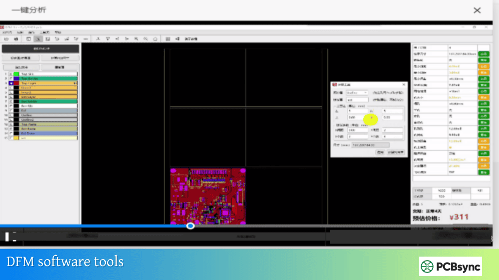
Should I invest in DFM software or rely on my manufacturer’s analysis?
Both approaches add value and work best in combination. Your own DFM software catches issues during design when changes are easy and cheap. You can iterate quickly without waiting for external feedback. Your manufacturer’s analysis validates your design against their specific capabilities and equipment—constraints that generic DFM tools might not capture. Consider in-house tools for continuous checking during development and manufacturer analysis for final validation before release. The small investment in both approaches pays back many times in avoided yield problems.
Building a Culture of Yield Excellence
The highest-yielding organizations don’t just run DFM checks—they build manufacturability thinking into their design culture. Engineers understand how their decisions affect production. Design reviews routinely include manufacturing representatives. Yield data flows back to design teams so they learn from production outcomes.
PCB yield improvement isn’t a one-time project. It’s a continuous process of learning what works, understanding what fails, and embedding that knowledge into design practices. The techniques described here—DFM for fabrication, DFA for assembly, systematic measurement, root cause analysis—form a framework for sustained yield improvement.
The boards that achieve 99% first-pass yield aren’t designed by engineers who got lucky. They’re designed by engineers who understand PCB manufacturing, collaborate with their production partners, and treat yield as a design requirement rather than a manufacturing problem. That’s the foundation of PCB yield improvement that actually works.
Inquire: Call 0086-755-23203480, or reach out via the form below/your sales contact to discuss our design, manufacturing, and assembly capabilities.
Quote: Email your PCB files to Sales@pcbsync.com (Preferred for large files) or submit online. We will contact you promptly. Please ensure your email is correct.
Notes: For PCB fabrication, we require PCB design file in Gerber RS-274X format (most preferred), *.PCB/DDB (Protel, inform your program version) format or *.BRD (Eagle) format. For PCB assembly, we require PCB design file in above mentioned format, drilling file and BOM. Click to download BOM template To avoid file missing, please include all files into one folder and compress it into .zip or .rar format.


