Inquire: Call 0086-755-23203480, or reach out via the form below/your sales contact to discuss our design, manufacturing, and assembly capabilities.
Quote: Email your PCB files to Sales@pcbsync.com (Preferred for large files) or submit online. We will contact you promptly. Please ensure your email is correct.
Notes: For PCB fabrication, we require PCB design file in Gerber RS-274X format (most preferred), *.PCB/DDB (Protel, inform your program version) format or *.BRD (Eagle) format. For PCB assembly, we require PCB design file in above mentioned format, drilling file and BOM. Click to download BOM template To avoid file missing, please include all files into one folder and compress it into .zip or .rar format.
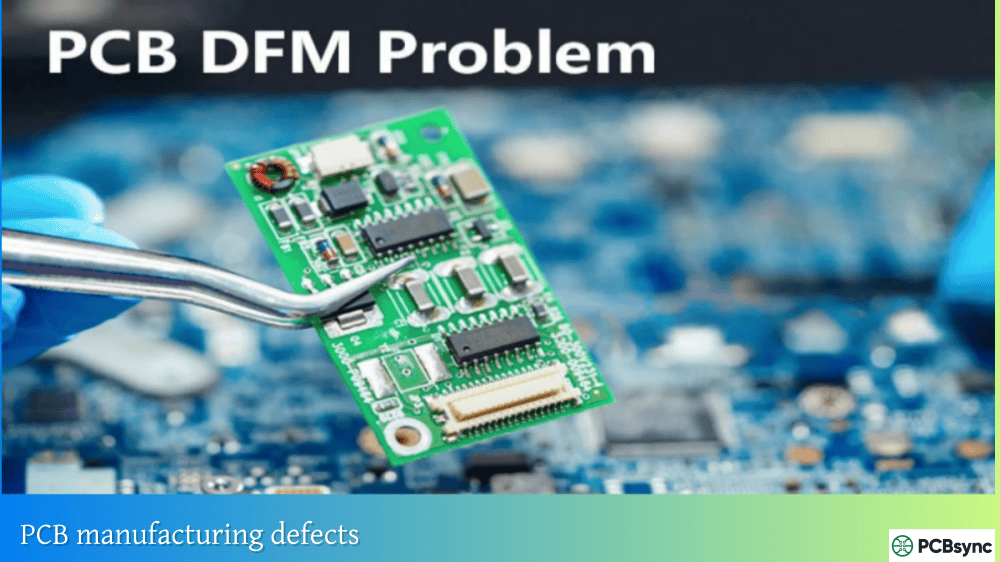
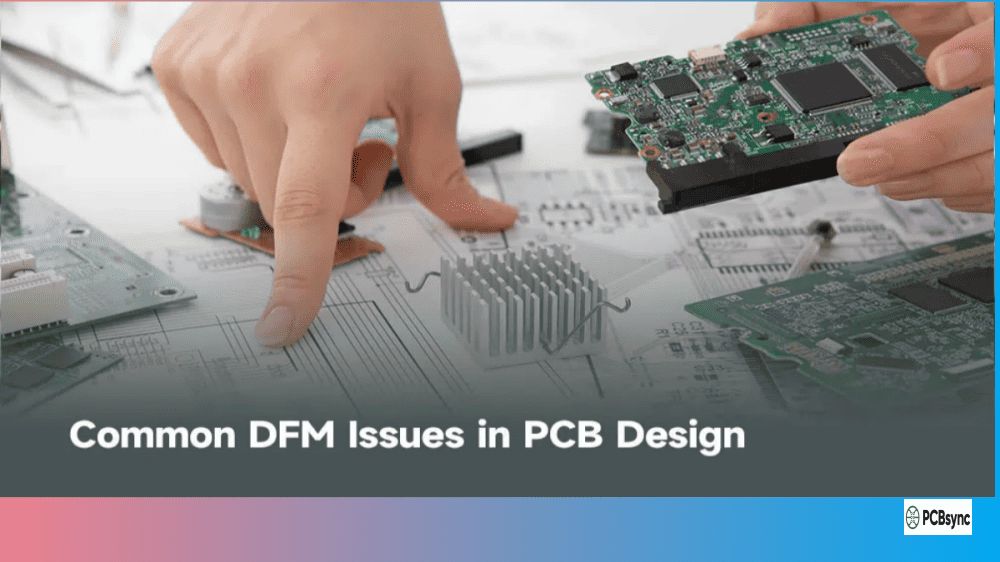
Every PCB designer has experienced that sinking feeling when a board comes back from manufacturing with unexpected issues—wrong footprints, untestable nets, assembly defects that could have been prevented. After twenty years in this industry, I’ve learned that most of these problems trace back to one root cause: designing in isolation without considering the full product lifecycle. DFX PCB methodology exists to prevent exactly this situation by embedding excellence into every design decision from day one.
DFX PCB isn’t just another acronym to memorize. It’s a comprehensive framework that transforms how we approach board design, ensuring products are manufacturable, testable, reliable, and cost-effective before they ever leave the CAD system. This guide breaks down the complete DFX framework and shows you how to implement it in your PCB projects.
Understanding DFX PCB: The Foundation of Design Excellence
DFX stands for Design for Excellence, where “X” represents any aspect of product development you want to optimize. In PCB design, DFX encompasses a collection of methodologies that address different stages of the product lifecycle—from fabrication through assembly, testing, and field operation.
The fundamental principle behind DFX PCB is straightforward: decisions made during design determine 70-80% of a product’s total cost and quality. Once a design is released to manufacturing, options for improvement narrow dramatically while costs for changes increase exponentially. DFX front-loads optimization, catching issues when fixes are cheap and easy.
Quality expectations: End users expect flawless products from day one
Cost pressure: Markets demand more functionality at lower prices
DFX PCB provides the framework to navigate these challenges systematically rather than reactively. Companies implementing comprehensive DFX practices report 20-30% reductions in time-to-market and significant improvements in first-pass yield.
The Cost of Ignoring DFX
Research consistently shows that 60% or more of quality issues and engineering changes result from design decisions. The cost to fix problems escalates dramatically as products progress through development:
Stage
Relative Cost to Fix
Design phase
1× (baseline)
Prototype
10×
Production ramp
100×
Field deployment
1,000×
A $10 design change becomes a $10,000 field recall. DFX PCB practices ensure problems are identified and resolved at the lowest-cost stage.
Core Components of the DFX PCB Framework
DFX PCB comprises several interrelated methodologies, each targeting specific aspects of excellence. Understanding how these components work together is essential for effective implementation.
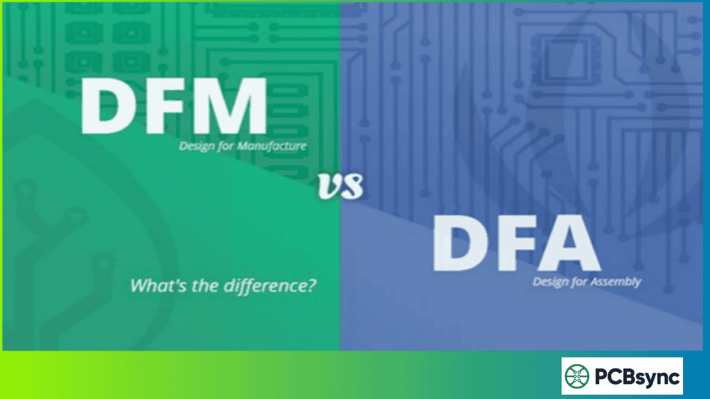
DFM: Design for Manufacturability
DFM ensures your PCB design aligns with fabrication capabilities and constraints. It’s the foundation of the DFX framework because if the bare board can’t be manufactured reliably, nothing else matters.
Key DFM considerations:
Parameter
Standard Capability
Advanced Capability
Minimum trace width
4-6 mil
2-3 mil
Minimum spacing
4-6 mil
2-3 mil
Minimum drill size
8-10 mil
4-6 mil (laser)
Via aspect ratio
8:1
10:1+
Copper weight
0.5-2 oz
3+ oz
Layer count
2-12
20+
DFM best practices:
Design to standard capabilities whenever performance permits
Maintain adequate annular rings (5 mil minimum, 8 mil recommended)
Balance copper distribution across layers to prevent warpage
Provide appropriate clearances from board edges
Use standard materials unless application requires otherwise
Avoid blind/buried vias unless HDI density demands them
DFM analysis should occur continuously during layout, not as a final check. Modern CAD tools provide real-time DFM feedback that catches issues as they’re created.
DFF: Design for Fabrication
DFF is a subset of DFM focusing specifically on bare board fabrication. It addresses the physical processes of lamination, drilling, plating, and etching.
Proper DFF implementation results in higher fabrication yields, more consistent quality, and lower per-board costs.
DFA: Design for Assembly
DFA optimizes your design for efficient component placement and soldering. With assembly often representing the largest portion of PCBA cost, DFA directly impacts bottom-line economics.
Component placement guidelines:
Spacing Type
Minimum
Recommended
SMD to SMD
0.5mm
1.0mm
SMD to through-hole
1.0mm
1.5mm
Component to board edge
3.0mm
5.0mm
Tall to short component
0.5mm
1.0mm
DFA best practices:
Orient polarized components consistently (all diodes same direction)
Align passive components on common axes (0° or 90°)
Keep components on one side when possible
Place heavy components on primary side
Provide adequate clearance for pick-and-place nozzles
Include fiducials for machine vision alignment
Design symmetric thermal connections for small passives (prevents tombstoning)
Effective DFA reduces assembly time, minimizes placement errors, and enables efficient automated production.
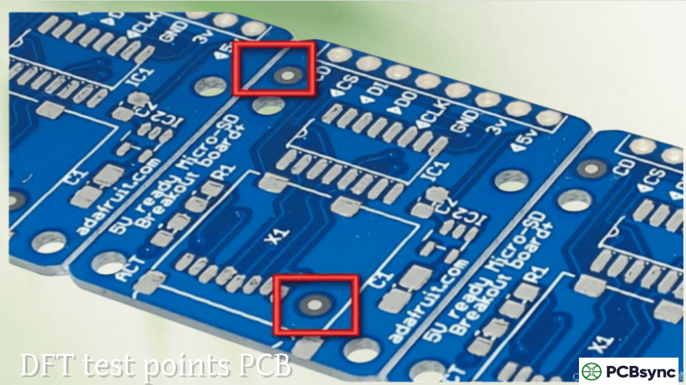
DFT: Design for Testability
DFT ensures your assembled boards can be efficiently verified for defects and functionality. Testing can consume 25-30% of total production cost, making DFT optimization highly impactful.
Test point requirements:
Test Method
Minimum Pad Size
Minimum Spacing
Bed-of-nails ICT
1.0mm (40 mil)
2.5mm (100 mil)
Flying probe
0.5mm (20 mil)
1.5mm (60 mil)
Manual probing
1.0mm (40 mil)
N/A
DFT best practices:
Provide one test point per net (target 95%+ coverage)
Place test points on single side (reduces fixture cost)
Maintain clearance from components and edges
Include JTAG connector for boundary scan capable devices
Provide access to critical signals for debug
Design for probe clearance (no tall components blocking access)
Distribute test points evenly (prevents board flex)
Boards designed with DFT in mind achieve faster fault detection, lower test costs, and easier field troubleshooting.
DFR: Design for Reliability
DFR focuses on ensuring products perform consistently throughout their intended lifecycle. Reliability problems discovered in the field are the most expensive to address.
Reliability considerations:
Factor
Design Impact
Thermal management
Component placement, via stitching, thermal relief
Mechanical stress
Mounting hole locations, component attachment
Environmental exposure
Material selection, conformal coating provisions
Component derating
Operating margin below maximum ratings
Failure mode analysis
FMEA during design review
DFR best practices:
Derate components to 60-80% of maximum ratings
Provide thermal relief for heat-generating components
Consider vibration and shock in component selection
Design for appropriate environmental conditions
Use proven materials with documented reliability data
Implement redundancy for critical functions
Account for aging effects over product lifetime
Investing in DFR during design is significantly cheaper than testing for reliability or addressing field failures.
Extended DFX PCB Methodologies
Beyond the core disciplines, several additional DFX methodologies address specific aspects of product excellence.
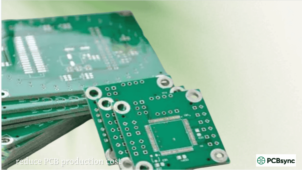
DFC: Design for Cost
DFC systematically optimizes design decisions to minimize total product cost without compromising functionality.
Cost reduction strategies:
Strategy
Implementation
Component standardization
Reduce unique part numbers
Layer count optimization
Use minimum layers meeting requirements
Standard materials
Avoid exotic laminates unless necessary
Panel utilization
Optimize board dimensions for efficient panelization
Via strategy
Through-hole vias cost less than blind/buried
Component selection
Choose cost-effective parts with multiple sources
DFC considers lifecycle cost, not just initial production cost. A slightly more expensive component with better reliability may reduce total cost through fewer field failures.
DFSC: Design for Supply Chain
DFSC ensures component availability and minimizes supply chain risk—lessons learned painfully during recent global shortages.
Supply chain considerations:
Risk Factor
Mitigation Strategy
Single source components
Qualify alternate sources
Long lead time parts
Identify early in design
End-of-life components
Monitor lifecycle status
Regional availability
Consider global sourcing
Minimum order quantities
Match to production volumes
DFSC best practices:
Verify component availability before design commitment
Prefer components with multiple manufacturers
Avoid end-of-life or NRND (not recommended for new design) parts
Consider lead times in project planning
Document approved manufacturer list (AML) with alternates
Monitor component lifecycle throughout product life
Designs optimized for supply chain resilience avoid costly production delays and emergency redesigns.
DFS: Design for Serviceability
DFS ensures products can be efficiently maintained, repaired, and updated throughout their operational life.
Serviceability features:
Feature
Benefit
Accessible test points
Enables field diagnostics
Replaceable modules
Simplifies repair
Clear labeling
Reduces service time
Standard connectors
Enables component swap
Diagnostic LEDs
Indicates system status
For products with extended service life or field-replaceable components, DFS significantly impacts total cost of ownership.
DFE: Design for Environment
DFE addresses environmental impact throughout the product lifecycle, increasingly important for regulatory compliance and corporate responsibility.
Environmental considerations:
Requirement
Implementation
RoHS compliance
Lead-free materials and processes
REACH compliance
Restricted substance documentation
WEEE compliance
Recyclability and proper disposal
Energy efficiency
Low-power design where applicable
Material selection
Avoid hazardous substances
DFE also encompasses design for recycling (DFRc) and design for disassembly (DFD), enabling end-of-life material recovery.
Many CMs offer DFX review services—use them. Their manufacturing expertise catches issues designers might miss.
DFX PCB Tools and Resources
Modern design tools include extensive DFX capabilities that automate many checks.
Design Software DFX Features
Tool
DFX Capabilities
Altium Designer
Built-in DFM/DFA rules, 3D clearance, testability analysis
Cadence Allegro
Constraint-driven design, manufacturing rules, DFT features
Mentor PADS
Design rule checking, assembly verification
KiCad
DRC with configurable rules, BOM management
Online DFX Analysis Tools
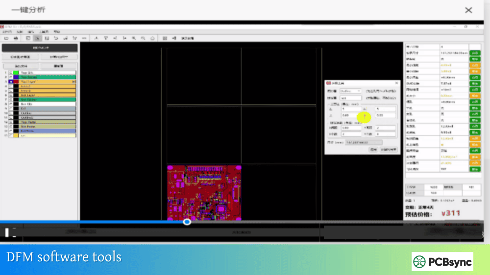
Several free tools provide DFX analysis:
JLCDFM (jlcdfm.com): Free web-based DFM/DFA analysis with interactive Gerber viewer
NextPCB HQDFM: Free online DFX verification with comprehensive checks
Sierra Circuits: DFM review service with engineering feedback
Industry Standards
These standards provide authoritative DFX guidance:
IPC-2221: Generic Standard on Printed Board Design—foundational design rules
IPC-2231: Design for Excellence Guidelines—comprehensive DFX framework
IPC-7351: Land Pattern Standard—component footprint guidelines
IPC-A-610: Acceptability of Electronic Assemblies—workmanship standards
IPC-6012: Qualification and Performance Specification—bare board requirements
Frequently Asked Questions About DFX PCB
What is the difference between DFM and DFX?
DFM (Design for Manufacturability) is a component of DFX (Design for Excellence). DFM specifically addresses bare board fabrication and production optimization. DFX is the broader framework encompassing DFM plus additional methodologies: DFA (assembly), DFT (testability), DFR (reliability), DFC (cost), DFSC (supply chain), and others. Think of DFX as the umbrella under which all “Design for X” methodologies reside. While DFM focuses on “can this board be manufactured?”, DFX asks the broader question: “will this product be excellent across all dimensions—manufacturability, assembly, testing, reliability, cost, and supply chain?” Implementing comprehensive DFX means addressing all these aspects systematically during design.
When should I start applying DFX principles in my design?
DFX should begin at project inception, not as a final review before manufacturing release. During requirements definition, establish reliability targets, cost constraints, and test strategies. During schematic capture, make component selections considering supply chain availability, cost targets, and reliability requirements—this is where DFSC and DFC have maximum impact. During layout, apply DFM rules continuously rather than checking only at completion. Before prototype release, conduct comprehensive DFX review with your PCB manufacturing partner. The fundamental principle is that design decisions determine 70-80% of product cost and quality, so DFX effectiveness correlates directly with how early it’s implemented. A DFX check at the end catches problems, but DFX mindset throughout prevents them.
How do I balance conflicting DFX requirements?
DFX trade-offs are inevitable. Increasing component spacing for DFA may compromise routing density (DFM concern). Adding test points for DFT requires board area that affects cost (DFC). Using premium components for DFR increases BOM cost. Resolution requires prioritization based on product requirements: medical devices prioritize DFR and DFT; consumer products may emphasize DFC and DFA; aerospace applications prioritize DFR with less cost sensitivity. Engage cross-functional teams early—manufacturing engineers, test engineers, and reliability engineers alongside designers. Document trade-off decisions and rationale. Modern CAD tools help by providing real-time feedback on multiple DFX parameters simultaneously. The goal isn’t perfect optimization of every aspect; it’s informed decisions that achieve overall product excellence given specific requirements and constraints.
What DFX checks should I request from my manufacturer?
Request comprehensive DFM/DFA analysis before committing to production. Specific checks should include: trace width and spacing verification against equipment capabilities; annular ring adequacy; drill aspect ratio feasibility; solder mask registration requirements; component spacing for pick-and-place equipment; thermal profile compatibility for reflow; test coverage analysis against available equipment. Ask about their DFX review process and typical findings—experienced CMs have institutional knowledge about common issues. Request feedback on your specific design, not just generic guidelines. Many CMs provide DFX services at no additional charge because catching issues before production benefits everyone. For critical products, consider paying for enhanced DFX review with detailed engineering feedback and recommendations.
How does DFX PCB affect product cost?
DFX directly impacts product cost in multiple ways. DFM optimization reduces fabrication cost by aligning designs with standard capabilities—exotic features like micro-vias or controlled impedance traces add cost. DFA optimization reduces assembly time and defect rates, lowering PCBA cost and rework expenses. DFT optimization reduces test time and fixture costs while improving yield. DFSC prevents costly production delays from component unavailability. DFR reduces warranty costs and field service expenses. Industry data suggests companies implementing comprehensive DFX achieve 20-40% cost reduction compared to designs developed without systematic DFX practices. The upfront investment in DFX analysis—whether through engineering time, software tools, or CM services—pays returns throughout product lifecycle. Most importantly, DFX prevents the most expensive costs: production delays, redesigns, and field failures.
Useful Resources for DFX PCB Implementation
These resources support engineers implementing DFX practices:
Industry Standards and Guidelines:
IPC-2231: Design for Excellence Guidelines—comprehensive industry standard for DFX implementation
IPC-2221B: Generic Standard on Printed Board Design—foundational design rules
IPC-7351C: Land Pattern Standard—component footprint guidelines
IPC-A-610: Acceptability of Electronic Assemblies—workmanship and inspection criteria
Design Tool Documentation:
Altium Designer DFM Documentation: Comprehensive guide to built-in DFM/DFA features
Cadence Allegro Manufacturing Rules: Constraint-driven design for manufacturability
Mentor DFM Analysis: Design verification tools and methodologies
Manufacturer Design Guides: Most PCB fabricators publish DFM guidelines specific to their capabilities
Component Engineering Resources:
Octopart (octopart.com): Component availability and lifecycle data
SiliconExpert: Component lifecycle management and obsolescence tracking
IHS Markit: Component database with supply chain intelligence
Making DFX PCB Part of Your Design Culture
DFX isn’t a checklist to complete—it’s a mindset that influences every design decision. Organizations that achieve true design excellence share common characteristics:
Cross-functional collaboration: Design engineers work closely with manufacturing, test, and quality teams throughout development, not just at handoff.
Continuous learning: Every production issue becomes a lesson that improves future designs. Post-mortems identify DFX gaps and refine guidelines.
Tool integration: DFX analysis tools are embedded in the design workflow, providing real-time feedback rather than end-of-process checks.
Manufacturing partnership: CMs are treated as partners contributing expertise, not vendors receiving completed designs.
Documentation discipline: DFX decisions and trade-offs are documented, creating institutional knowledge that survives personnel changes.
DFX PCB isn’t about achieving perfection—it’s about systematic excellence that produces better products, faster development, and lower costs. Every design benefits from DFX thinking, whether it’s a simple two-layer board or a complex HDI assembly.
The investment in understanding and implementing DFX principles pays dividends on every project. Boards go through manufacturing smoothly, yields are high, products perform reliably, and costs stay under control. That’s the excellence the “X” represents—and it’s achievable with the systematic approach this framework provides.
Inquire: Call 0086-755-23203480, or reach out via the form below/your sales contact to discuss our design, manufacturing, and assembly capabilities.
Quote: Email your PCB files to Sales@pcbsync.com (Preferred for large files) or submit online. We will contact you promptly. Please ensure your email is correct.
Notes: For PCB fabrication, we require PCB design file in Gerber RS-274X format (most preferred), *.PCB/DDB (Protel, inform your program version) format or *.BRD (Eagle) format. For PCB assembly, we require PCB design file in above mentioned format, drilling file and BOM. Click to download BOM template To avoid file missing, please include all files into one folder and compress it into .zip or .rar format.


