Inquire: Call 0086-755-23203480, or reach out via the form below/your sales contact to discuss our design, manufacturing, and assembly capabilities.
Quote: Email your PCB files to Sales@pcbsync.com (Preferred for large files) or submit online. We will contact you promptly. Please ensure your email is correct.
Notes: For PCB fabrication, we require PCB design file in Gerber RS-274X format (most preferred), *.PCB/DDB (Protel, inform your program version) format or *.BRD (Eagle) format. For PCB assembly, we require PCB design file in above mentioned format, drilling file and BOM. Click to download BOM template To avoid file missing, please include all files into one folder and compress it into .zip or .rar format.
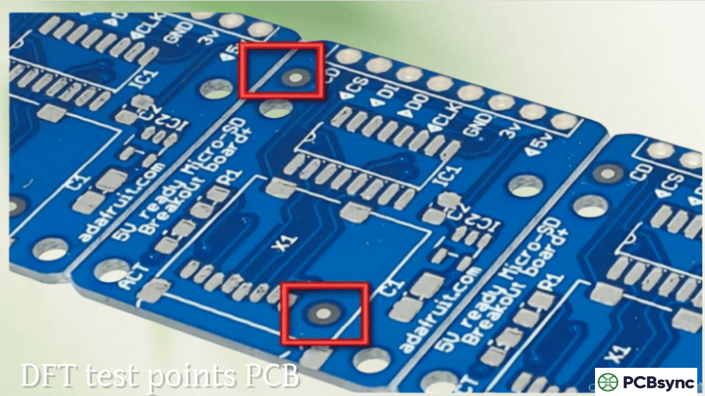
I’ve lost count of how many times I’ve seen a beautifully routed PCB come back from assembly with defects that could have been caught—if only the board had proper test access. The reality is that testing can account for up to 30% of your total production cost. When you design DFT test points PCB layouts correctly from the start, you slash that cost significantly while catching defects before they become field failures.
Design for Testability (DFT) isn’t an afterthought—it’s a fundamental design discipline that determines whether your board can be efficiently tested during manufacturing. This guide covers everything you need to know about test point design, from sizing and spacing to placement strategies that work with both ICT fixtures and flying probe systems.
Test points are designated locations on your PCB where test equipment can make electrical contact to verify circuit functionality. They’re the physical interface between your design and the test systems that validate it. Without adequate test points, even the most sophisticated test equipment becomes useless.
DFT test points PCB design enables three critical capabilities:
Observability allows you to measure what’s happening inside your circuit—voltage levels, signal integrity, component values. Without test points on key nets, these measurements become impossible.
Controllability lets you inject signals or power into specific nodes during testing. This is essential for isolating faults and verifying component functionality.
Fault coverage measures what percentage of potential defects your testing can actually detect. Industry targets typically aim for 90-95% fault coverage on critical designs. Inadequate test points directly limit this coverage.
According to IPC surveys, companies investing in proper DFT see 20-30% reduction in time to market due to streamlined testing and debugging. The math is simple: time spent adding test points during design costs far less than time spent troubleshooting untestable boards in production.
Test Point Types and When to Use Each
Not all test points are created equal. Understanding the options helps you choose the right approach for your specific testing needs.
For most production testing scenarios, dedicated test pads are preferred because they provide the most reliable probe contact. Vias work when space is tight, but their smaller size reduces contact reliability. Component pads can serve double duty for flying probe testing but shouldn’t be your primary strategy for ICT.
Test Point Sizing Specifications
Size matters enormously for test points. Too small, and probes can’t make reliable contact. Too large, and you waste precious board real estate. Here are the specifications that work across most test systems:
Recommended Test Point Dimensions
Parameter
ICT (Bed-of-Nails)
Flying Probe
Manual Probing
Minimum Pad Diameter
0.9mm (35 mil)
0.5mm (20 mil)
1.0mm (40 mil)
Preferred Pad Diameter
1.0mm (40 mil)
0.75mm (30 mil)
1.5mm (60 mil)
Optimal Pad Diameter
1.5mm (60 mil)
1.0mm (40 mil)
2.0mm (80 mil)
For ICT fixtures, I recommend 1.0mm (40 mil) minimum pad diameter. This provides adequate contact area for standard 100-mil probes while remaining practical for most board densities. If you can spare the space, 1.5mm pads significantly improve contact reliability.
Flying probe systems can work with smaller pads—down to 0.5mm (20 mil)—because the probes are precisely positioned by software. However, smaller targets increase test time as the system needs more careful positioning.
Pad Shape Considerations
Circular pads are standard, but square pads offer approximately 27% more surface area for the same footprint width. This extra area can improve contact reliability, particularly for ICT fixtures where probe alignment has some tolerance. If your CAD tool supports it and your fab house doesn’t object, square pads are worth considering.
Test Point Spacing Requirements
Spacing between test points determines which probe sizes your fixture can use. Larger probes are more reliable and less expensive—but they need more room.
Center-to-Center Spacing
Recommended Probe Size
Reliability
Cost
2.54mm (100 mil)
100 mil probe
Excellent
Low
1.78mm (70 mil)
75 mil probe
Good
Moderate
1.27mm (50 mil)
50 mil probe
Fair
Higher
0.99mm (39 mil)
39 mil probe
Marginal
High
The golden rule: keep DFT test points PCB spacing at 2.54mm (100 mil) minimum whenever possible. This allows use of standard 100-mil probes, which are the most reliable and economical option for ICT fixtures.
When 100-mil spacing isn’t achievable, 70-mil spacing with 75-mil probes is a reasonable compromise. Going below 50-mil spacing should be avoided unless absolutely necessary—the thinner probes required are more prone to bending and wear, increasing fixture maintenance costs.
Test Point Placement Strategies
Where you place test points matters as much as how you size them. Poor placement leads to limited access, fixture complications, and incomplete fault coverage.
Single-Sided vs. Double-Sided Access
Whenever possible, locate all test points on one side of the board—typically the bottom (secondary side). Single-sided test access dramatically simplifies fixture design and reduces cost. Double-sided fixtures require precise alignment between top and bottom probe plates, adding complexity and expense.
If top-side test points are unavoidable, reserve them for non-critical nets where occasional contact issues won’t compromise test coverage.
Edge Clearance Requirements
Test points too close to board edges create problems for fixture clamping and probe access. Maintain these minimum clearances:
Feature
Minimum Clearance
Preferred Clearance
Board Edge to Test Point
3.0mm (125 mil)
3.8mm (150 mil)
Board Edge to Component
3.0mm (125 mil)
5.0mm (200 mil)
Tooling Hole to Test Point
3.2mm (125 mil)
4.0mm (160 mil)
Component Height Considerations
Tall components create “no-fly zones” where probes cannot access nearby test points. On the probed side, components taller than 6.4mm (255 mil) require fixture cutouts and significantly larger keep-out areas around adjacent test points.
Component Height
Keep-out from Test Points
< 2.6mm (100 mil)
2.0mm (80 mil)
2.6-6.4mm (100-255 mil)
3.0mm (120 mil)
> 6.4mm (255 mil)
5.0mm (200 mil) + fixture cutout
Place tall components on the non-probed side whenever possible. If that’s not feasible, cluster test points away from tall component areas.
Distribution and Coverage
Test points should be distributed evenly across the board surface. Concentrated test points in one area create high mechanical stress during fixture activation, potentially causing board flex or warpage.
Target at least one test point per signal net. For power nets, allocate approximately 10% of ground nodes as dedicated ground test points, distributed evenly across the board. These ground references are essential for accurate measurements.
Tooling Holes for ICT Fixtures
Test fixtures align to your PCB using tooling holes. Without proper tooling, probe registration suffers and contact reliability drops.
Tooling Hole Requirements
Place at least two unplated tooling holes in diagonally opposite corners of the board. Standard diameter is 3.2mm (125 mil) with tight tolerance (±0.05mm).
Critical guidelines:
Position holes asymmetrically to prevent backward insertion
Maintain 3.2mm annular clearance around each hole—no components or test points in this zone
For panelized boards, include tooling holes on breakaway rails
Consider adding a third tooling hole for large boards or designs requiring precise alignment. The third hole prevents any rotation error that two-hole systems might allow.
Different test methods have different requirements. Optimize your DFT test points PCB design for the methods you’ll actually use.
In-Circuit Testing (ICT)
ICT uses bed-of-nails fixtures where hundreds of spring-loaded probes contact the board simultaneously. This method excels at high-volume production but requires upfront fixture investment.
Key ICT design requirements:
Test points on every net requiring measurement
100-mil minimum spacing (70-mil acceptable with care)
Flying probe systems use movable probes controlled by software—no custom fixture required. This makes them ideal for prototypes and low-volume production.
Design considerations for flying probe:
Smaller test points acceptable (0.5mm minimum)
Tighter spacing tolerated (but increases test time)
Both sides accessible (system can flip board)
Clean, flat pad surfaces essential for reliable contact
Avoid solder mask over test points
Boundary Scan (JTAG)
For complex digital designs, boundary scan testing through JTAG interfaces complements physical test points. This technique tests interconnections between ICs without physical probes.
Include a JTAG header near the board edge for easy access. Standard headers use 2.54mm pitch with 4-5 pins (TCK, TMS, TDI, TDO, and optionally TRST).
Common DFT Test Point Mistakes to Avoid
After reviewing hundreds of designs, these errors appear repeatedly:
Insufficient test point coverage: Designers often add test points to obvious nets but miss secondary signals. Every net that could fail needs access—not just power and ground.
Test points under components: Placing test pads directly beneath component bodies makes them inaccessible. Always verify clearance from component outlines.
Ignoring fixture constraints: Designing without knowing your test system’s capabilities leads to untestable boards. Get the fixture specifications before you start layout.
Solder mask over test points: Test points must have solder mask openings to allow probe contact. Verify your mask layer explicitly exposes all test points.
Clustered test point placement: Dense test point areas cause probe interference and board stress. Distribute points evenly across the board surface.
Useful DFT Resources and Tools
Here are resources that will help you implement effective DFT in your designs:
What is the minimum test point size for ICT testing?
For ICT bed-of-nails fixtures, minimum test point diameter is 0.9mm (35 mil), though 1.0mm (40 mil) is strongly recommended for reliable contact. Flying probe systems can work with smaller pads down to 0.5mm (20 mil), but contact reliability decreases with size.
How many test points should a PCB have?
Ideally, every signal net should have at least one accessible test point. For comprehensive fault coverage (90%+), this typically means one test point per net, plus additional ground reference points (approximately 10% of total ground nodes) distributed across the board.
Can vias be used as test points?
Yes, exposed vias can serve as test points, but with limitations. Via test points have smaller contact areas than dedicated pads, reducing probe reliability. For ICT, via holes should be at least 0.5mm diameter with exposed annular rings. Tented or plugged vias cannot be used for testing.
What’s the difference between DFT and DFM?
DFM (Design for Manufacturability) ensures your board can be fabricated and assembled correctly. DFT (Design for Testability) ensures your board can be tested effectively after assembly. They’re complementary disciplines—a board needs both to succeed in production.
Should test points be on the top or bottom of the PCB?
Bottom-side test points are preferred because single-sided test fixtures are simpler and less expensive. If your design requires double-sided testing, put critical nets on the bottom and reserve top-side access for secondary measurements.
Final Thoughts
Effective DFT test points PCB design isn’t complicated, but it does require planning from the earliest stages of your project. Know your test method before you start layout. Understand your fixture manufacturer’s constraints. Add test points during schematic capture, not as an afterthought in layout.
The time you invest in proper DFT pays dividends throughout production—faster test development, higher fault coverage, fewer escapes to the field, and lower overall manufacturing cost. Your production team will thank you, and so will your bottom line.
Meta Description Suggestion:
DFT test points PCB design guide: Learn test point sizing, spacing, and placement for ICT and flying probe testing. Includes specifications tables, common mistakes to avoid, and practical tips from a PCB engineer.
Inquire: Call 0086-755-23203480, or reach out via the form below/your sales contact to discuss our design, manufacturing, and assembly capabilities.
Quote: Email your PCB files to Sales@pcbsync.com (Preferred for large files) or submit online. We will contact you promptly. Please ensure your email is correct.
Notes: For PCB fabrication, we require PCB design file in Gerber RS-274X format (most preferred), *.PCB/DDB (Protel, inform your program version) format or *.BRD (Eagle) format. For PCB assembly, we require PCB design file in above mentioned format, drilling file and BOM. Click to download BOM template To avoid file missing, please include all files into one folder and compress it into .zip or .rar format.


