Inquire: Call 0086-755-23203480, or reach out via the form below/your sales contact to discuss our design, manufacturing, and assembly capabilities.
Quote: Email your PCB files to Sales@pcbsync.com (Preferred for large files) or submit online. We will contact you promptly. Please ensure your email is correct.
Notes: For PCB fabrication, we require PCB design file in Gerber RS-274X format (most preferred), *.PCB/DDB (Protel, inform your program version) format or *.BRD (Eagle) format. For PCB assembly, we require PCB design file in above mentioned format, drilling file and BOM. Click to download BOM template To avoid file missing, please include all files into one folder and compress it into .zip or .rar format.
After 15 years of designing circuit boards for everything from consumer electronics to aerospace systems, I’ve learned one painful truth: passing lab tests doesn’t guarantee field success. I’ve watched beautifully designed PCBs fail spectacularly because we didn’t account for real-world conditions. That’s exactly why DFR PCB reliability has become the cornerstone of my design philosophy.
Design for Reliability (DFR) isn’t just another buzzword. It’s a systematic approach that integrates reliability considerations into every stage of the PCB design lifecycle. When done right, it prevents the kind of failures that lead to costly recalls, damaged reputations, and sleepless nights.
Design for Reliability represents a proactive engineering methodology focused on predicting and eliminating potential failure points before a single board reaches production. Unlike reactive quality control that catches defects after pcb manufacturing, DFR addresses failure risks during the design phase when changes are cheapest and most effective.
At its core, DFR PCB reliability ensures that your product performs its specified function within its intended environment for the entire expected lifetime. This involves analyzing thermal behavior, mechanical stress, component tolerances, and environmental factors long before fabrication begins.
The Business Case for DFR Implementation
The economics here are compelling. Studies estimate that over half of electronic component failures stem from thermal stress alone. When you factor in field failure costs, warranty claims, and brand damage, investing in DFR during design becomes a no-brainer. A design change that costs $100 during schematic review might cost $10,000 after prototyping and $1,000,000 after product launch.
Core DFR Principles Every PCB Engineer Should Follow
Conservative Design Margins
Think of conservative design as a safety factor for your PCB. I always apply two fundamental principles here:
Component Derating: Never run components at their maximum rated specifications. A capacitor rated at 16V should ideally see no more than 10V in your design. A microcontroller rated for 85°C operation should be thermally managed to stay below 70°C. This buffer accounts for manufacturing variations, aging, and worst-case operating conditions.
Generous Copper Weight: When it comes to copper and reliability, more is better. Over time, copper can degrade, especially under high voltage stress. Thicker copper layers and wider traces improve thermal dissipation, reduce resistance heating, and provide margin against manufacturing variations.
Component Selection for DFR PCB Reliability
Choosing the right component is perhaps the most impactful DFR practice you can implement. Here’s what I evaluate for every critical component:
Selection Criteria
Design Consideration
Impact on Reliability
Temperature Range
Match to worst-case operating environment plus margin
Prevents thermal failures in field
Voltage Derating
Select ratings 20-50% above maximum expected stress
Guards against transients and aging
Package Type
Larger packages for critical applications
Better thermal performance, easier inspection
Manufacturer Quality
Source from reputable vendors with quality certifications
Consistent performance, fewer counterfeit risks
End-of-Life Status
Avoid obsolete or last-time-buy components
Ensures long-term production capability
For harsh environment applications, don’t hesitate to upgrade from commercial-grade to industrial or military-grade components. The cost difference is typically minimal compared to field failure consequences.
Implementing FMEA for PCB Reliability
Failure Mode and Effects Analysis (FMEA) forms the analytical backbone of any serious DFR program. This systematic methodology helps identify potential failure modes, their causes, and their effects before problems manifest in production or the field.
The FMEA Process for PCB Design
The FMEA workflow I follow involves rating each potential failure mode across three dimensions:
Severity (S): How serious are the consequences if this failure occurs? A scale of 1-10, where 10 represents catastrophic failure affecting safety.
Occurrence (O): How likely is this failure mode to happen? Higher numbers indicate greater probability.
Detection (D): How likely is current testing to catch this failure before it reaches customers? Lower numbers mean better detection capability.
The Risk Priority Number (RPN) equals S × O × D. Failure modes with high RPNs demand immediate design attention.
Failure Mode
Typical Cause
Severity
Occurrence
Detection
RPN
Recommended Action
Solder Joint Crack
Thermal cycling
7
6
4
168
Increase pad size, avoid fine pitch
Via Barrel Failure
Thermal stress
8
4
5
160
Increase plating thickness
Component Burnout
Inadequate derating
9
3
3
81
Apply 50% derating factor
ESD Damage
Handling issues
6
5
6
180
Add protection circuits, improve handling
Moisture Ingress
Poor conformal coating
7
4
5
140
Specify coating coverage requirements
Thermal Management Strategies for DFR PCB Reliability
Heat is the silent killer of electronic components. Every 10°C rise in junction temperature roughly halves the expected lifetime of a semiconductor device. Effective thermal management isn’t optional—it’s essential for DFR PCB reliability.
PCB Thermal Design Best Practices
Component Placement Optimization
Distribute high-power components uniformly across the board to prevent localized hotspots. Maintain minimum 3mm spacing between heat-generating components. Position temperature-sensitive ICs away from hot components, ideally in cooler board regions like the bottom section where natural convection helps.
Thermal Via Implementation
Thermal vias transfer heat from surface layers to internal copper planes or the bottom side of the board. For components with exposed thermal pads, I typically use a via field with 0.3mm diameter vias on 1mm centers. Fill vias with thermally conductive epoxy or cap them with copper to prevent solder wicking during assembly.
Copper Pour Strategies
Large copper pours act as heat spreaders, distributing thermal energy across greater surface area. Connect heat-generating component pads to ground planes using multiple vias. Use thermal relief patterns around solder points to facilitate assembly while maintaining adequate heat transfer.
IPC Standards and DFR PCB Reliability Requirements
Understanding IPC class requirements is fundamental to designing reliable PCBs. These standards establish acceptance criteria based on your product’s intended application and reliability requirements.
For DFR PCB reliability in critical applications, always design to Class 3 requirements. The tighter tolerances and stricter acceptance criteria directly translate to longer service life and fewer field failures.
Key IPC Standards for PCB Reliability
IPC-2221: Generic Standard on Printed Board Design—covers material selection, conductor spacing, and thermal management guidelines
IPC-6012: Qualification and Performance Specification for Rigid Printed Boards—defines performance requirements including thermal shock resistance and solderability
IPC-A-610: Acceptability of Electronic Assemblies—the inspection standard covering solder joint quality, component placement, and cleanliness
IPC-J-STD-001: Requirements for Soldered Electrical and Electronic Assemblies—soldering materials, processes, and acceptance criteria
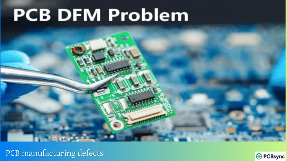
Common PCB Failure Modes and Prevention Strategies
Understanding how PCBs fail is essential for preventing failures. Here are the most common failure modes I encounter and proven prevention strategies:
Solder Joint Failures
Solder joints represent the most vulnerable interconnection in any PCBA. Thermal cycling causes expansion and contraction at different rates between the PCB, solder, and components, eventually leading to fatigue cracking.
Prevention Approaches:
Use SAC305 or similar high-reliability solder alloys
Avoid fine-pitch components (0.5mm and below) where possible
Increase pad sizes to allow proper fillet formation
Interconnect defects in multilayer boards often occur at plated through-holes, where thermal stress can cause barrel cracking or separation from internal layers.
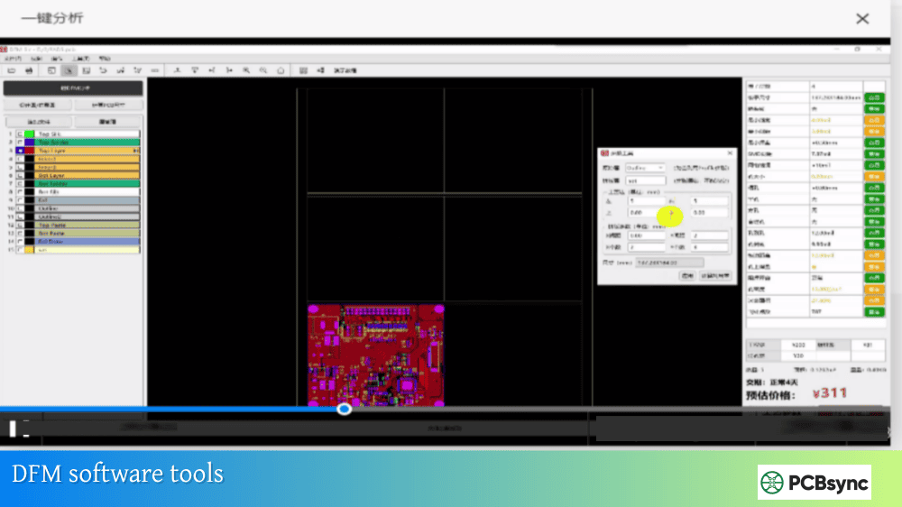
Modern simulation tools allow virtual reliability testing before committing to fabrication. Essential simulations include:
Thermal Analysis: Software like ANSYS, SolidWorks Thermal, or Cadence Celsius identifies hotspots, predicts temperature distribution, and evaluates cooling effectiveness before prototyping.
Signal Integrity Analysis: Validates that high-speed signals maintain proper characteristics under worst-case conditions, preventing intermittent failures.
Mechanical Stress Analysis: Predicts board flex, vibration response, and thermal-mechanical stress concentrations that could lead to failures.
Combining simulation with physical testing guarantees reliable thermal performance, optimized cooling designs, and improved long-term DFR PCB reliability.
Useful Resources and Databases for PCB Reliability
Here are essential resources I reference regularly for DFR work:
Industry Standards and Guidelines
IPC Standards Library: www.ipc.org — Complete catalog of PCB design, fabrication, and assembly standards
JEDEC Standards: www.jedec.org — Component packaging and reliability testing standards
MIL-STD Specifications: Available through Defense Logistics Agency for military and aerospace requirements
Component Reliability Data
SN29500 Component Reliability Database: Standard reference for component failure rates
MIL-HDBK-217F: Reliability Prediction of Electronic Equipment—classic failure rate calculation methodology
Manufacturer Reliability Reports: Most major component suppliers publish reliability data upon request
Design Tools and Calculators
IPC-2152 Current Capacity Calculator: Trace width calculations for thermal reliability
Saturn PCB Toolkit: Free tool for via current capacity, trace temperature rise, and other reliability calculations
Cadence Allegro X with Celsius Solver: Integrated thermal analysis in PCB design flow
Industry Organizations
IPC (Association Connecting Electronics Industries): Training, certification, and standards
IEEE Electronics Packaging Society: Academic and industry research
Frequently Asked Questions About DFR PCB Reliability
What is the difference between DFR and DFM in PCB design?
Design for Reliability (DFR) focuses on ensuring long-term product performance and preventing field failures throughout the expected service life. Design for Manufacturability (DFM) addresses production efficiency and yield optimization during manufacturing. While DFM asks “can we build this efficiently?”, DFR asks “will this survive its intended lifetime?” Both are essential—a manufacturable design that fails in the field serves nobody well.
How early in the design process should DFR be implemented?
DFR should begin at concept phase and continue through every stage. The earlier you implement reliability considerations, the lower the cost of addressing them. During schematic design, focus on component derating and selection. During layout, address thermal management and spacing requirements. Before fabrication release, perform FMEA analysis and simulation verification.
What is the most common cause of PCB field failures?
Solder joint failures from thermal cycling represent the most frequent field failure mode, followed by component failures from inadequate derating and environmental degradation from moisture or contamination. Proper thermal management, conservative component selection, and appropriate protective coatings address these three primary failure mechanisms.
How do I choose between IPC Class 2 and Class 3 for my design?
Choose Class 3 when continuous operation is critical, failure consequences are severe, or the operating environment is harsh. Medical devices, aerospace systems, and industrial control equipment typically require Class 3. Choose Class 2 for commercial and industrial products where extended life and reliability matter but brief service interruptions are acceptable. Consumer electronics often use Class 1 or Class 2.
Can simulation replace physical reliability testing?
Simulation complements but cannot replace physical testing. Simulations excel at identifying design weaknesses, comparing alternatives, and optimizing designs before committing to hardware. However, physical testing validates real-world performance, uncovers failure modes not predicted by models, and provides qualification evidence for customers and regulatory bodies. The most robust DFR programs combine both approaches.
Building Your DFR Process
Implementing DFR PCB reliability doesn’t require massive upfront investment. Start with these practical steps:
Establish Component Standards: Create approved parts lists with reliability requirements. Specify derating factors, acceptable manufacturers, and temperature ratings.
Implement Design Reviews: Add reliability checkpoints to your design review process. Ensure thermal analysis and FMEA are completed before layout release.
Capture Failure Data: Track field failures systematically. Analyze root causes and feed lessons learned back into design guidelines.
Invest in Simulation: Modern thermal and signal integrity tools pay for themselves by preventing costly prototype iterations.
Partner with Your Manufacturer: Your PCB fabricator and assembler have valuable reliability insights. Involve them early to leverage their process knowledge.
The best designs I’ve produced resulted from treating reliability as a design parameter from day one, not an afterthought to be tested in at the end. When you build DFR PCB reliability into your design culture, field failures become rare exceptions rather than routine problems.
Your customers may never notice the reliability work you’ve done—and that’s exactly the point. The best reliability engineering is invisible, quietly ensuring that products perform flawlessly for years beyond their warranty period.
Inquire: Call 0086-755-23203480, or reach out via the form below/your sales contact to discuss our design, manufacturing, and assembly capabilities.
Quote: Email your PCB files to Sales@pcbsync.com (Preferred for large files) or submit online. We will contact you promptly. Please ensure your email is correct.
Notes: For PCB fabrication, we require PCB design file in Gerber RS-274X format (most preferred), *.PCB/DDB (Protel, inform your program version) format or *.BRD (Eagle) format. For PCB assembly, we require PCB design file in above mentioned format, drilling file and BOM. Click to download BOM template To avoid file missing, please include all files into one folder and compress it into .zip or .rar format.


