Inquire: Call 0086-755-23203480, or reach out via the form below/your sales contact to discuss our design, manufacturing, and assembly capabilities.
Quote: Email your PCB files to Sales@pcbsync.com (Preferred for large files) or submit online. We will contact you promptly. Please ensure your email is correct.
Notes: For PCB fabrication, we require PCB design file in Gerber RS-274X format (most preferred), *.PCB/DDB (Protel, inform your program version) format or *.BRD (Eagle) format. For PCB assembly, we require PCB design file in above mentioned format, drilling file and BOM. Click to download BOM template To avoid file missing, please include all files into one folder and compress it into .zip or .rar format.
DFMA in PCB Design: Combining Manufacturing & Assembly Optimization
I’ve reviewed thousands of PCB designs over my career, and the pattern is unmistakable: boards designed without manufacturing and assembly in mind consistently cost more, take longer to produce, and have higher defect rates. DFMA PCB practices exist to break this cycle by integrating fabrication and assembly considerations directly into the design process—not as an afterthought, but as a fundamental design driver.
DFMA PCB methodology recognizes a simple truth: 70-80% of a product’s manufacturing cost is determined during design. Once you’ve committed to a certain layer count, component selection, and board layout, your cost trajectory is largely fixed. The engineers assembling your board can’t undo design decisions that make their job harder. DFMA front-loads these considerations, optimizing designs before they ever reach the factory floor.
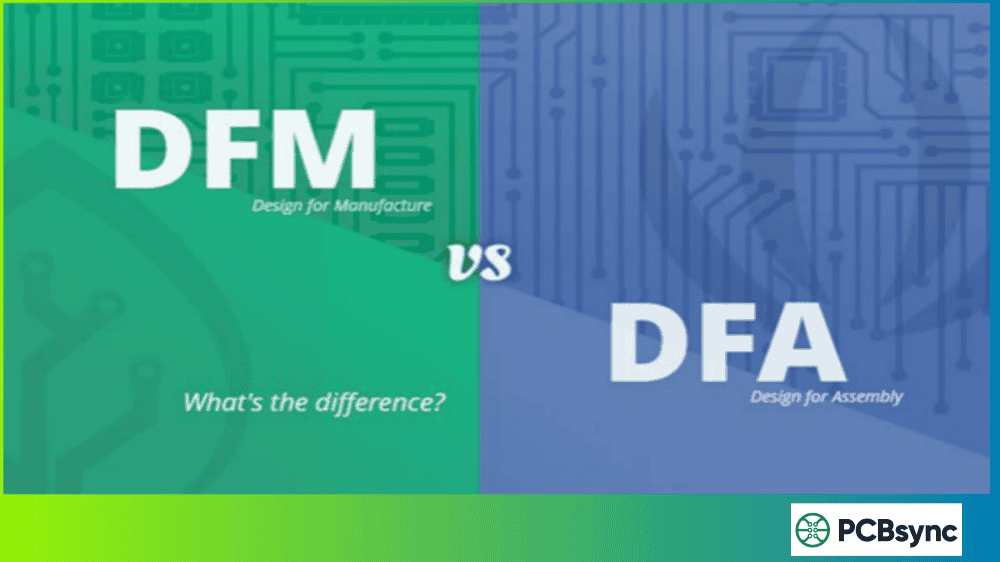
DFMA stands for Design for Manufacturing and Assembly—a combined methodology that optimizes PCB designs for both bare board fabrication (DFM) and component assembly (DFA). Rather than treating these as separate concerns, DFMA PCB recognizes that decisions affecting one inevitably impact the other.
The methodology originated from academic research by Geoffrey Boothroyd and Peter Dewhurst in the 1980s, who developed systematic approaches to predict and reduce assembly time and cost during design. Their work earned the U.S. National Medal of Technology and Innovation in 1991, validating DFMA’s profound impact on manufacturing efficiency.
The Two Pillars of DFMA PCB
Design for Manufacturing (DFM): Focuses on bare board fabrication—ensuring your PCB can be reliably produced within standard manufacturing capabilities. DFM addresses trace widths, via structures, copper balancing, material selection, and dozens of other parameters that affect fabrication yield and cost.
Design for Assembly (DFA): Focuses on component placement and soldering—ensuring your PCBA can be efficiently populated with minimum errors. DFA addresses component selection, placement orientation, spacing, pad design, and process compatibility.
When combined, DFMA PCB delivers synergistic benefits: designs that are easy to fabricate are typically easier to assemble, and assembly-friendly designs often require fabrication features that align with standard manufacturing capabilities.
Why DFMA PCB Matters Now
Modern electronics face intensifying pressures that make DFMA essential:
Challenge
DFMA Impact
Cost pressure
Systematic optimization reduces total product cost 20-40%
Time-to-market
Fewer iterations and production delays accelerate delivery
Companies implementing comprehensive DFMA practices report typical outcomes including 20-50% part count reduction, 10-30% assembly time reduction, and significant reductions in tooling and supply chain costs.
Core DFMA PCB Principles
DFMA methodology rests on foundational principles that guide all design decisions.
Minimize Part Count
Reducing component count is DFMA’s most powerful lever. Every component you eliminate removes:
Direct material cost
Placement operation
Solder joint (potential failure point)
Inspection point
Inventory line item
Potential supply chain risk
Practical part reduction strategies:
Strategy
Example
Consolidate resistor values
Use two 10kΩ in series instead of adding unique 20kΩ
Select integrated ICs
Replace discrete logic gates with single IC
Eliminate protection redundancy
Remove redundant ESD diodes if IC has internal protection
Combine functions
Use MCU with integrated peripherals vs. discrete components
Question every passive
Challenge whether each capacitor and resistor is truly necessary
Part count reduction has cascading benefits: fewer components means fewer placement operations, fewer feeder setups, shorter assembly time, and lower defect probability.
Standardize Components
Component standardization amplifies DFMA benefits across the entire supply chain:
Benefits of standardization:
Bulk purchasing power reduces per-unit cost
Reduced inventory complexity and carrying cost
Simplified logistics and procurement
Increased availability from multiple sources
Reduced feeder changeovers during assembly
Easier training for assembly operators
Standardization targets:
Component Type
Standardization Approach
Resistors
Limit to common values (1%, E96 series when possible)
Capacitors
Standardize on package sizes (0402, 0603, 0805)
Connectors
Use same family across products
Fasteners
Limit screw types and sizes
Passives
Prefer standard footprints over custom
When component selection begins, ask: “Does a standard part exist that meets requirements?” Only specify custom or specialty components when standard options genuinely cannot satisfy functional needs.
Design for Automated Assembly
Manual assembly introduces variability, increases cost, and doesn’t scale. DFMA PCB prioritizes designs compatible with automated pick-and-place and reflow processes:
Automation-friendly design features:
Consistent component orientation (all ICs pin-1 same direction)
Adequate spacing for pick-and-place nozzles
Standard component packages supported by feeders
Fiducials for machine vision alignment
Single-sided placement when possible
Compatible with standard reflow profiles
Dual-sided assembly increases costs 20-30% due to additional process steps, handling, and potential for first-side component damage during second-side reflow.
Minimize Assembly Operations
Each assembly operation adds time, cost, and defect opportunity. DFMA PCB minimizes operations by:
Reducing process steps:
SMT-only designs eliminate wave soldering
Single-side placement eliminates board flip
Selecting reflow-compatible through-hole (pin-in-paste) when THT is required
Simulate routing before committing to higher counts
Consider if signals truly require internal routing
Evaluate if impedance control is necessary
Question whether dedicated power layers are required
A 4-layer board costs 30-50% more than 2-layer but provides significant routing and signal integrity benefits. The jump from 4 to 6 layers often has smaller proportional cost impact while enabling substantially more complex designs.
Select Appropriate Via Structures
Via selection significantly impacts both cost and manufacturing complexity:
Via Type
Cost Impact
When to Use
Through-hole
1.0× (baseline)
Default choice; simplest manufacturing
Blind
1.5-2.0×
Only when routing density absolutely requires
Buried
2.0-3.0×
HDI designs; sequential lamination
Microvia
2.0-3.0×
Fine-pitch BGA breakout; laser drilling
Via optimization guidelines:
Default to through-hole vias
Use blind/buried only when design cannot be achieved otherwise
Consider via-in-pad only for fine-pitch components
Maintain standard aspect ratios (8:1 or less for reliability)
Each advanced via type requires additional manufacturing steps, tighter process control, and increased inspection—all adding cost.
Design Within Standard Capabilities
Manufacturing capability tiers have significant cost implications:
Tombstoning—where small passive components stand upright during reflow—is almost always caused by asymmetric thermal conditions between the two pads. Equal pad sizes and balanced copper connections prevent this common defect.
Thermal Management for Assembly
Thermal considerations affect both soldering success and long-term reliability:
Thermal relief design:
Use thermal relief patterns on plane-connected pads
Maintain consistent copper around small component pads
Position heat-generating components for airflow
Include thermal vias under power components
Reflow compatibility:
Verify all components are reflow-rated
Group components with similar thermal requirements
Consider thermal mass distribution across board
Avoid large ground plane connections without relief
Systematic DFMA analysis catches issues before they become production problems.
When to Perform DFMA Analysis
DFMA should be integrated throughout design, not just at the end:
Design Phase
DFMA Activities
Concept
Define manufacturing constraints, target cost
Schematic
Component selection, standardization review
Layout
Placement optimization, DFM rule checking
Review
Comprehensive DFMA analysis with CM
Prototype
Validate assumptions, capture lessons
Production
Monitor yields, refine guidelines
The earlier issues are identified, the cheaper they are to fix. A design change during schematic capture costs virtually nothing; the same change after prototype fabrication may cost thousands.
DFMA Checklist for PCB Designs
Use this checklist during design review:
Part Count and Standardization:
Challenge necessity of each component
Consolidate values where possible
Standardize package sizes
Minimize unique part numbers
Verify component availability
Fabrication (DFM):
Layer count justified by requirements
Trace width/spacing within standard capability
Via structures appropriate (prefer through-hole)
Copper balanced across layers
Standard materials specified
Assembly (DFA):
Components on single side when possible
Consistent orientation throughout
Adequate spacing for automation
Thermal balance on passive components
Fiducials included for machine vision
Panel design optimized
Process Compatibility:
All components reflow-compatible
Mixed technology minimized
Manual operations eliminated where possible
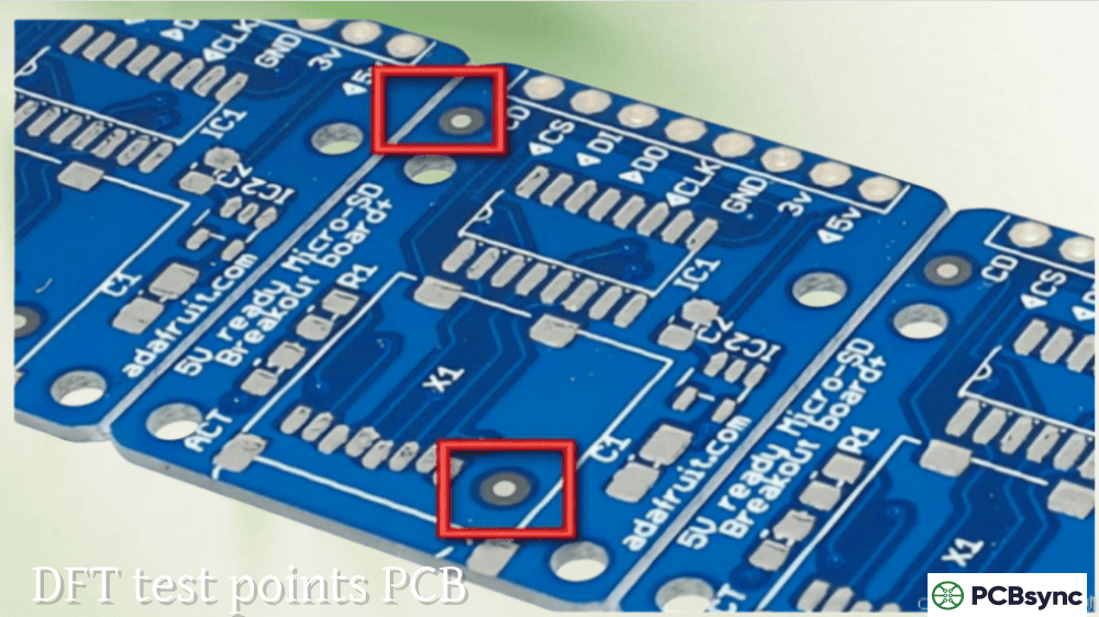
Test access provided
Working with Your Contract Manufacturer
Your CM is a critical DFMA partner. Effective collaboration includes:
Request from CM:
Capability documents (minimums and standards)
Assembly equipment specifications
Preferred component packages
Panel size and tooling requirements
DFM/DFA review services
Provide to CM:
Complete design files
BOM with approved alternates
Assembly drawings
Special requirements documentation
Target volumes and quality class
Many CMs offer free DFMA review—use this service. Their manufacturing expertise catches issues designers might miss.
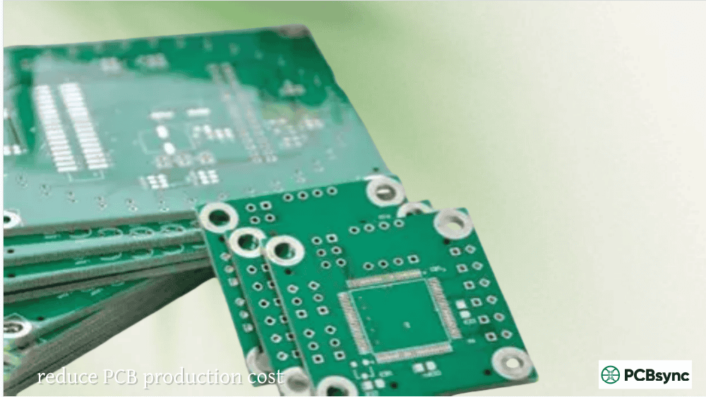
DFMA PCB Cost Impact Analysis
Quantifying DFMA benefits helps justify investment in proper design practices.
Component cost typically dominates, making part count reduction the highest-impact DFMA strategy. However, assembly labor and yield improvements can provide significant savings, especially at volume.
Quantifying DFMA Savings
Typical DFMA optimization results:
Metric
Typical Improvement
Part count
20-50% reduction
Assembly time
10-30% reduction
Fabrication cost
15-25% reduction
Defect rate
30-50% reduction
Time to market
20-30% faster
For a $10 assembly, 25% cost reduction represents $2.50 per unit. At 10,000 units, that’s $25,000 saved—typically far exceeding DFMA analysis investment.
Common DFMA PCB Mistakes to Avoid
These frequently encountered errors undermine manufacturing efficiency:
Excessive Layer Count
Mistake: Specifying more layers than the design requires.
Impact: 30-50% cost increase per layer pair; longer lead times.
Prevention: Route simulation before committing; question whether signals truly need internal layers.
Non-Standard Component Selection
Mistake: Specifying exotic packages, custom values, or single-source components.
Prevention: Include minimum three global fiducials; local fiducials for fine-pitch components.
Frequently Asked Questions About DFMA PCB
What is the difference between DFM and DFMA?
DFM (Design for Manufacturability) focuses specifically on bare board fabrication—ensuring your PCB can be reliably produced by addressing trace widths, via structures, material selection, and other fabrication parameters. DFMA (Design for Manufacturing and Assembly) combines DFM with DFA (Design for Assembly), which addresses component placement, orientation, spacing, and soldering considerations. DFMA is the comprehensive methodology that optimizes both fabrication and assembly together. This combined approach recognizes that decisions affecting bare board fabrication inevitably impact assembly, and vice versa. For example, via-in-pad decisions affect both fabrication (filled/capped vias cost more) and assembly (unfilled vias can cause solder wicking). DFMA addresses these interconnected concerns holistically rather than as separate optimizations.
How much can DFMA reduce PCB costs?
DFMA typically reduces total product cost 20-40% compared to designs developed without systematic optimization. Specific improvements vary by product complexity and starting point, but typical results include 20-50% part count reduction, 10-30% assembly time reduction, 15-25% fabrication cost reduction, and 30-50% defect rate reduction. The most significant savings often come from part count reduction, which eliminates direct material cost plus associated placement, inspection, and inventory costs. A Logitech case study reported 40% part count reduction and 50% assembly time reduction through DFMA redesign. Cost impact scales with production volume—savings compound with each unit produced. For a $10 assembly with 25% cost reduction at 100,000 units, total savings reach $250,000.
When should I perform DFMA analysis in the design process?
DFMA should be integrated throughout design, not performed only at the end. During concept phase, establish manufacturing constraints and target costs. During schematic capture, apply component selection and standardization criteria—this is when part count reduction has maximum impact. During layout, apply DFM rules continuously and optimize placement for assembly. Before prototype release, conduct comprehensive DFMA review with your PCB manufacturing partner. After prototype, capture lessons learned and refine guidelines. The fundamental DFMA principle is that 70-80% of manufacturing cost is determined during design, making early optimization essential. Changes during schematic capture are essentially free; changes after fabrication can cost thousands in redesign, re-tooling, and production delays.
Should I use single-sided or double-sided PCB assembly?
Single-sided assembly is always preferred from a DFMA perspective when component density permits. Single-sided assembly requires only one reflow pass, eliminates risks associated with bottom-side components (falling off during second reflow, thermal cycling stress), reduces handling operations, and typically costs 20-30% less than double-sided assembly. However, component density requirements often necessitate both sides. When using double-sided assembly, follow these DFMA guidelines: place heavy and tall components on the primary side only; limit bottom-side components to lightweight SMT parts that won’t fall during reflow; consider component height restrictions based on selective solder or second reflow requirements; and plan for appropriate glue dots if bottom components must survive wave soldering. The decision should be based on rigorous analysis of whether density truly requires both sides, not default assumption.
How do I convince management to invest in DFMA practices?
Present DFMA as risk reduction and cost avoidance, not additional expense. Quantify potential savings using typical DFMA outcomes (20-40% cost reduction) applied to your projected production volumes. A $10 assembly at 10,000 units with 25% savings represents $25,000—typically far exceeding DFMA implementation cost. Highlight schedule benefits: DFMA reduces iterations, avoiding costly redesign cycles that delay time-to-market. Reference industry data showing 60% of quality issues and engineering changes result from design decisions, making design-phase optimization essential. Start with a pilot project to demonstrate measurable results. Many contract manufacturers offer free DFMA review services—leverage these to show specific improvement opportunities at no cost. Frame DFMA as competitive advantage: companies implementing systematic DFMA consistently outperform competitors on cost, quality, and delivery.
Useful Resources for DFMA PCB Implementation
These resources support engineers implementing DFMA practices:
Industry Standards:
IPC-2221B: Generic Standard on Printed Board Design—foundational DFM requirements
IPC-2231: Design for Excellence Guidelines—comprehensive DFX framework including DFMA
IPC-7351C: Land Pattern Standard—component footprint guidelines for assembly
IPC-A-610: Acceptability of Electronic Assemblies—workmanship standards
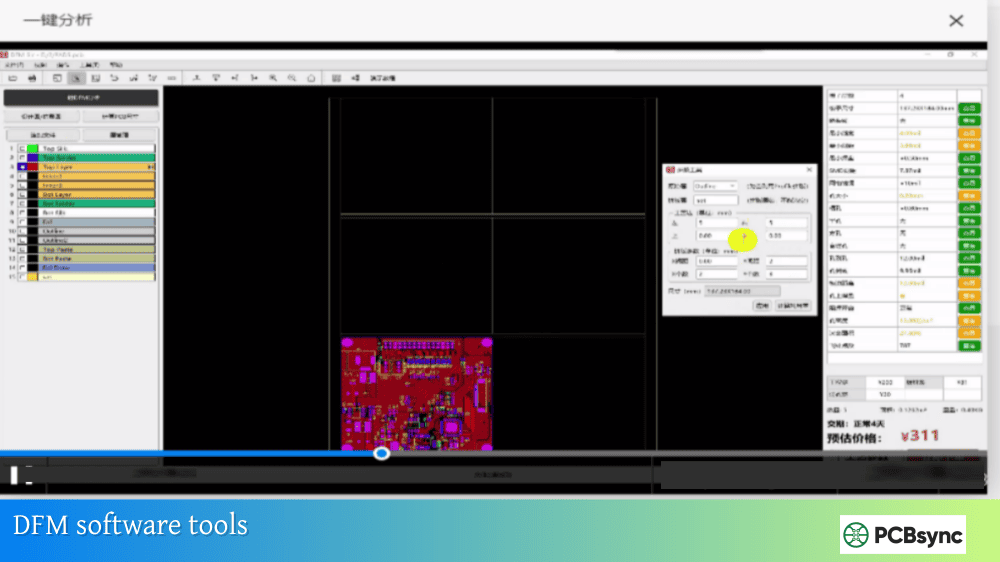
DFMA Software and Tools:
Boothroyd Dewhurst DFMA Software (dfma.com): Original DFMA methodology tools for concurrent costing and design optimization
DFMPro: Integrated DFM analysis for major CAD platforms
Valor NPI: Comprehensive DFM/DFA analysis platform
Sierra Circuits: Free DFM check with engineering feedback
Design Tool Resources:
Altium Designer: Built-in DFM/DFA rules and real-time checking
Cadence Allegro: Constraint Manager with manufacturing rules
OrCAD: Integrated DFM checking with manufacturer specification import
Educational Resources:
Boothroyd Dewhurst Resources (dfma.com/resources): Case studies, white papers, and DFMA methodology documentation
IPC Designer Certification (CID/CID+): Industry certification covering DFMA principles
University of Florida DFMA Tips: Comprehensive design guidelines reference
Component Engineering:
Octopart (octopart.com): Component availability and alternate sourcing
SiliconExpert: Component lifecycle and obsolescence tracking
Digi-Key/Mouser: Standard component catalogs with datasheet access
Making DFMA PCB a Design Culture
Effective DFMA implementation requires more than checklists—it requires cultural commitment to manufacturing-aware design:
Build cross-functional teams: Include manufacturing and test engineers in design reviews from the beginning, not just at handoff. Their production floor experience catches issues designers miss.
Learn from every build: Conduct post-production reviews capturing manufacturing feedback. Document issues and incorporate lessons into design guidelines for future projects.
Invest in tools: Modern CAD software includes powerful DFMA features. Enable real-time DFM/DFA checking; configure rules based on actual manufacturer capabilities; use these tools throughout design, not just at completion.
Partner with manufacturers: Treat your CM as a design partner, not a vendor. Their expertise in manufacturing thousands of designs provides invaluable optimization insight. Request and use their DFMA review services.
Measure and improve: Track DFMA metrics—part count, assembly time, defect rates, cost per unit. Use data to demonstrate improvement and identify remaining opportunities.
DFMA PCB isn’t about constraining creativity—it’s about channeling design decisions toward outcomes that work well in manufacturing. The best designs are not just electrically correct; they’re optimized for the realities of production. That optimization starts with understanding DFMA principles and applying them systematically throughout the design process.
The investment in DFMA thinking pays returns on every project: lower costs, faster time-to-market, higher quality, and fewer production surprises. That’s the combined power of manufacturing and assembly optimization working together from design day one.
Inquire: Call 0086-755-23203480, or reach out via the form below/your sales contact to discuss our design, manufacturing, and assembly capabilities.
Quote: Email your PCB files to Sales@pcbsync.com (Preferred for large files) or submit online. We will contact you promptly. Please ensure your email is correct.
Notes: For PCB fabrication, we require PCB design file in Gerber RS-274X format (most preferred), *.PCB/DDB (Protel, inform your program version) format or *.BRD (Eagle) format. For PCB assembly, we require PCB design file in above mentioned format, drilling file and BOM. Click to download BOM template To avoid file missing, please include all files into one folder and compress it into .zip or .rar format.


