Inquire: Call 0086-755-23203480, or reach out via the form below/your sales contact to discuss our design, manufacturing, and assembly capabilities.
Quote: Email your PCB files to Sales@pcbsync.com (Preferred for large files) or submit online. We will contact you promptly. Please ensure your email is correct.
Notes: For PCB fabrication, we require PCB design file in Gerber RS-274X format (most preferred), *.PCB/DDB (Protel, inform your program version) format or *.BRD (Eagle) format. For PCB assembly, we require PCB design file in above mentioned format, drilling file and BOM. Click to download BOM template To avoid file missing, please include all files into one folder and compress it into .zip or .rar format.
DFM vs DFA: Key Differences and When to Apply Each in PCB Design
DFM vs DFA in PCB design: Learn the key differences between Design for Manufacturing and Design for Assembly, when to apply each, and get practical checklists from a PCB engineer’s perspective. Includes comparison tables and resources.
As a PCB engineer with years spent troubleshooting manufacturing delays and assembly headaches, I can tell you that understanding DFM vs DFA isn’t just academic—it’s the difference between a smooth production run and costly respins. Both methodologies aim to optimize your PCB design, but they tackle completely different stages of the production pipeline. Getting them confused, or worse, ignoring one entirely, is a mistake I’ve seen derail too many projects.
This guide breaks down the core differences between Design for Manufacturing (DFM) and Design for Assembly (DFA), explains when to apply each, and provides actionable checklists you can start using today.
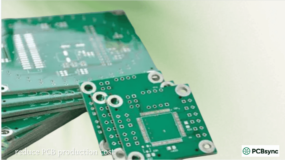
Design for Manufacturing (DFM) focuses on optimizing your PCB design so the bare board can be fabricated without issues. We’re talking about the actual circuit board itself—the substrate, copper traces, vias, and layers—before any components get soldered on.
DFM addresses questions like: Can my fabricator actually produce 4-mil traces? Are my drill holes within their capability? Will my layer stackup cause delamination issues?
When I run a DFM check, I’m essentially validating that my design respects the physical limitations of the manufacturing equipment. Every fab house has different capabilities, and what works at one shop might be impossible at another.
Core DFM Parameters to Check
The fabrication process involves etching copper, drilling holes, plating vias, and applying surface finishes. Each step has tolerances that your design must respect:
Trace width and spacing are usually the first things that get flagged. Most standard fabs can handle 5-6 mil traces reliably, but pushing to 3-4 mils requires more advanced equipment and drives up costs. The same applies to spacing between traces—insufficient clearance leads to shorts or etching problems.
Via design matters more than many engineers realize. The aspect ratio (board thickness divided by drill diameter) determines whether plating can fully coat the hole barrel. Most manufacturers recommend keeping this ratio below 8:1. For a 1.6mm board, that means your smallest via should be at least 0.2mm.
Annular ring size directly affects yield. If your drill registration is off by even a few mils, an undersized annular ring can cause breakout or tangency—conditions where the hole touches or exceeds the pad boundary. IPC standards specify minimum annular rings based on product class.
Solder mask clearance needs adequate spacing to prevent bridging between pads. A typical minimum is 3-4 mils expansion around pads, but this varies with manufacturer capability.
What Is DFA in PCB Design?
Design for Assembly (DFA) picks up where DFM leaves off. Once you have a bare board, DFA ensures that components can be placed, soldered, and tested efficiently. This is about the assembly process—pick-and-place machines, reflow ovens, wave soldering, and inspection.
DFA considerations include: Can my pick-and-place machine handle these component packages? Is there enough clearance for the nozzle to drop parts? Will reflow cause tombstoning on my 0402 capacitors?
The assembly phase is typically the most time-consuming and expensive part of PCBA production. A board that passes DFM with flying colors can still become a nightmare during assembly if DFA principles were ignored.
Core DFA Parameters to Check
Assembly involves component placement, soldering, testing, and often rework. Each step has requirements your layout must accommodate:
Component spacing determines whether pick-and-place machines can accurately position parts without collision. Maintain at least 50 mils clearance around components for automated assembly. For hand rework, you’ll want even more.
Fiducial markers are essential for optical alignment in automated assembly. Global fiducials (at least two on opposite corners) help the machine locate the board, while local fiducials assist with fine-pitch component placement.
Pad sizing and geometry directly affect solder joint quality. Pads that are too small cause insufficient solder fillets; pads that are too large can lead to component shifting during reflow. Following IPC-7351B footprint standards is your safest bet.
Component orientation should be consistent across your design. All polarized components facing the same direction reduces placement errors and speeds up visual inspection. ICs should have pin 1 marked clearly and consistently.
Thermal considerations matter for reflow soldering. Components with large thermal masses (like heavy connectors or big QFN packages) need proper thermal relief and may require adjusted reflow profiles.
DFM vs DFA: Understanding the Key Differences
Here’s where the rubber meets the road. While both DFM and DFA aim to make production smoother, they focus on fundamentally different aspects of your PCB project.
Tombstoning, solder bridges, inaccessible test points
When to Run
Before Gerber release for fab
Before BOM and placement files release
Who Performs Check
PCB designer, fabricator
PCB designer, assembly house
Cost Impact
Affects bare board cost and yield
Affects assembly time, labor, and rework rate
The timing distinction is critical. DFM parameters are essentially locked once fabrication begins—you can’t change your layer stackup or via sizes after the board is made. DFA considerations offer slightly more flexibility since you can sometimes adjust component selection or placement even after initial board fabrication, though this is obviously not ideal.
When to Apply DFM in Your Design Process
DFM analysis shouldn’t be a one-time check at the end of your design. The most effective approach is running DFM validation at multiple stages:
During Schematic and Component Selection
Before you even start layout, think about manufacturability. If you’re specifying 01005 passives, confirm your fab and assembly partners can handle them. If your design requires HDI with microvias, make sure that capability exists at your target manufacturers.
During Floorplanning
This is when you determine layer count, approximate trace widths, and via strategies. Running initial DFM checks here prevents fundamental changes later. Decisions like whether to use blind/buried vias or stick with through-holes have massive manufacturability implications.
Before Design Rule Check (DRC)
Configure your CAD tool’s design rules based on your manufacturer’s capabilities. This ensures DRC catches violations in real-time during routing. Most ECAD tools like Altium, Cadence, or KiCad allow importing manufacturer-specific rule files.
Before Gerber Generation
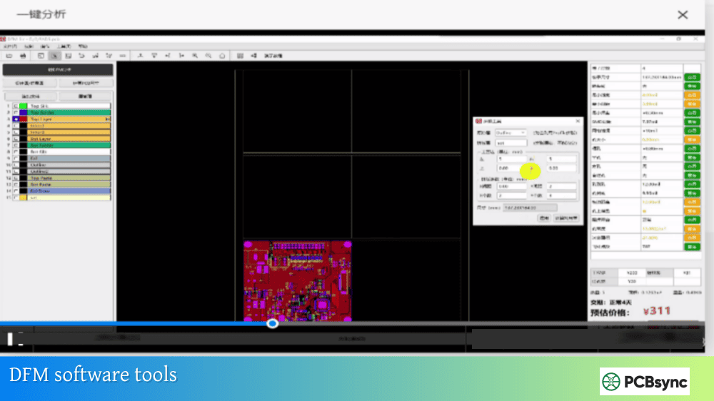
This is your final DFM gate. Run comprehensive checks against your fabricator’s capability list. Many manufacturers offer free DFM review services—take advantage of them. Catching issues here costs nothing; catching them after board fab costs serious money.
DFA considerations should run parallel to DFM, with particular attention during layout:
During Component Placement
This is DFA ground zero. Every component you place should be evaluated for assembly accessibility. Questions to ask: Can the pick-and-place nozzle reach this part? Is there clearance for solder paste stencil alignment? Can rework technicians access this component if needed?
When Defining Pad Geometry
Pad shapes and sizes directly impact solder joint formation. Use manufacturer-recommended footprints from IPC-7351B or component datasheets. Consider thermal balance—mismatched pad sizes on passive components cause tombstoning.
During Panelization Planning
How boards are arranged on a panel affects assembly efficiency. V-scoring vs. tab routing impacts edge clearances. Breakaway tab placement shouldn’t interfere with edge components or connectors.
Before Generating Assembly Files
Verify your BOM is clean, centroid files are accurate, and pick-and-place data matches your design. Include clear assembly drawings with polarity markings, first article inspection notes, and any special handling instructions.
DFM vs DFA: Comparison of Check Items
To give you a practical reference, here’s what each methodology typically examines:
DFM Check Items
DFA Check Items
Trace width and spacing
Component-to-component clearance
Via drill size and aspect ratio
Fiducial marker placement
Annular ring dimensions
Pad-to-pad spacing for soldering
Solder mask clearance and expansion
Component height restrictions
Copper-to-edge clearance
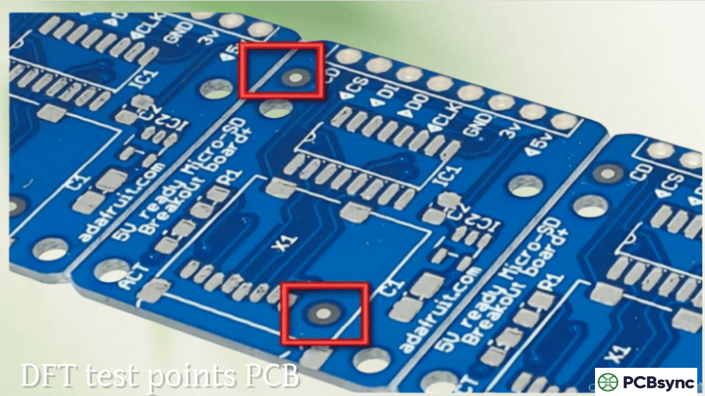
Test point accessibility
Layer stackup and material selection
Thermal relief on pads
Silkscreen line width and placement
Polarity and orientation markings
Drill-to-copper spacing
Stencil aperture design
Acid traps and copper slivers
Pick-and-place nozzle clearance
Surface finish specification
Wave soldering direction (THT)
DFMA: Combining Both Approaches
You’ll often see the term DFMA (Design for Manufacturing and Assembly) used to describe an integrated approach. This makes sense because optimizing for fabrication without considering assembly—or vice versa—leaves gaps.
In practice, DFMA means running both DFM and DFA checks iteratively throughout your design process. Some considerations overlap: for example, via-in-pad designs affect both fabrication (requiring filled and planarized vias) and assembly (preventing solder wicking).
The most effective teams include fabricators and assemblers early in the design cycle. Getting their input during schematic review or initial floorplanning prevents expensive changes downstream.
Common DFM and DFA Mistakes to Avoid
After reviewing thousands of designs, certain errors appear repeatedly:
Ignoring manufacturer capabilities is the number one mistake. Designing 3-mil traces when your fab’s standard capability is 5-mil forces either a more expensive process or a redesign. Always get your manufacturer’s capability matrix upfront.
Insufficient spacing for assembly causes more rework than almost any other issue. Cramming components tight saves board space but creates soldering headaches. Leave breathing room, especially around fine-pitch parts.
Missing or improperly placed fiducials slow down assembly significantly. Automated lines rely on these reference marks. Without them, manual alignment is required—expensive and error-prone.
Inconsistent component orientation increases inspection time and assembly errors. Standardize directions for all similar component types.
Neglecting thermal management in layout leads to assembly defects. Large ground planes or heavy copper pours can act as heat sinks, preventing proper solder reflow.
Useful Resources for DFM and DFA
Here are some resources I’ve found valuable for deepening your DFM and DFA knowledge:
Most major PCB manufacturers also offer free DFM review services with orders. Take advantage of these—they’re checking your design against their specific capabilities.
Frequently Asked Questions
What is the main difference between DFM and DFA?
DFM focuses on the fabrication of the bare PCB (traces, vias, layers, materials), while DFA focuses on the assembly process (component placement, soldering, testing). DFM ensures the board can be manufactured; DFA ensures components can be assembled onto it efficiently.
Should I run DFM or DFA first in my design process?
Both should run in parallel, but DFM considerations typically come first since layer stackup, trace widths, and via structures are fundamental decisions that must be made early. DFA checks become more relevant once component placement begins.
Can my design pass DFM but fail DFA?
Absolutely. A board might be perfectly manufacturable as a bare PCB but have assembly issues like insufficient component spacing, missing fiducials, or poor pad geometry that causes soldering defects. This is why both checks are necessary.
What does DFMA mean and when should I use it?
DFMA stands for Design for Manufacturing and Assembly—it’s an integrated approach combining both DFM and DFA principles. Use DFMA when you want a comprehensive analysis covering the entire production process from bare board to finished assembly.
How much do DFM and DFA issues affect costs?
Industry estimates suggest that 60-80% of product costs are determined by design decisions. DFM/DFA issues caught after production starts can add 15-20% to final PCB costs through respins, rework, and yield losses. Catching them during design is essentially free.
Final Thoughts
Understanding DFM vs DFA isn’t about choosing one over the other—it’s about applying both at the right stages of your design process. DFM ensures your bare board can be fabricated reliably and economically. DFA ensures that board can be assembled efficiently with high yield.
The best approach is working closely with your PCB manufacturing partners from the earliest design stages. Get their capability matrices, understand their processes, and design accordingly. The time invested upfront pays dividends in faster production, lower costs, and fewer late-night calls about yield problems.
Run both checks iteratively throughout your design cycle, not just at the end. Your future self—and your production team—will thank you.
Meta Description Suggestion:
DFM vs DFA in PCB design: Learn the key differences between Design for Manufacturing and Design for Assembly, when to apply each, and get practical checklists from a PCB engineer’s perspective. Includes comparison tables and resources.
Inquire: Call 0086-755-23203480, or reach out via the form below/your sales contact to discuss our design, manufacturing, and assembly capabilities.
Quote: Email your PCB files to Sales@pcbsync.com (Preferred for large files) or submit online. We will contact you promptly. Please ensure your email is correct.
Notes: For PCB fabrication, we require PCB design file in Gerber RS-274X format (most preferred), *.PCB/DDB (Protel, inform your program version) format or *.BRD (Eagle) format. For PCB assembly, we require PCB design file in above mentioned format, drilling file and BOM. Click to download BOM template To avoid file missing, please include all files into one folder and compress it into .zip or .rar format.


