Inquire: Call 0086-755-23203480, or reach out via the form below/your sales contact to discuss our design, manufacturing, and assembly capabilities.
Quote: Email your PCB files to Sales@pcbsync.com (Preferred for large files) or submit online. We will contact you promptly. Please ensure your email is correct.
Notes: For PCB fabrication, we require PCB design file in Gerber RS-274X format (most preferred), *.PCB/DDB (Protel, inform your program version) format or *.BRD (Eagle) format. For PCB assembly, we require PCB design file in above mentioned format, drilling file and BOM. Click to download BOM template To avoid file missing, please include all files into one folder and compress it into .zip or .rar format.
PCB Design for Manufacturing (DFM): Complete Guide to Reduce Costs & Errors
After twenty years of designing PCBs across consumer electronics, aerospace, and medical devices, I’ve learned one lesson repeatedly: designs that ignore manufacturability pay the price in delays, rework costs, and failed production runs. DFM PCB principles aren’t optional extras—they’re fundamental to getting boards built right the first time at reasonable cost. Studies show that more than half of PCB production delays trace directly back to DFM issues that could have been prevented during design.
This guide covers everything you need to implement effective DFM PCB practices: the principles behind manufacturability, specific design rules with real numbers, common errors to avoid, and practical checklists that will save your projects from expensive surprises.
DFM PCB—Design for Manufacturing applied to printed circuit boards—is the practice of optimizing your board design for efficient, reliable, and cost-effective production. It means considering fabrication and assembly constraints during the design phase, not as an afterthought when files go to the manufacturer.
The concept seems obvious, yet countless designs arrive at fabrication facilities with issues that require engineering queries, redesigns, or compromised specifications. Every iteration costs time and money. Worse, designs that slip through with marginal manufacturability produce boards with lower yields, higher defect rates, and reduced reliability.
The Real Cost of Ignoring DFM
When DFM principles are ignored, the consequences compound:
Immediate costs:
Engineering queries delay production start
Design respins require complete rework
Rush fees to recover lost schedule time
Scrap from boards that fail manufacturing
Hidden costs:
Lower production yields increase per-board cost
Field failures from marginal manufacturing quality
Strained manufacturer relationships
Delayed time-to-market
A well-optimized DFM PCB design can reduce manufacturing costs by 20-40% compared to designs that simply meet minimum specifications without optimization. Those savings come from higher yields, fewer engineering interventions, and efficient use of manufacturing panel space.
Benefits of Proper DFM Implementation
When DFM PCB practices are applied consistently, projects benefit from:
Benefit
Impact
Fewer design iterations
Reduces engineering time and NRE costs
Higher manufacturing yields
Lowers per-unit production cost
Faster time-to-market
Eliminates delays from manufacturability issues
Improved reliability
Designs within process margins perform better
Better manufacturer relationships
Easier quotes, priority treatment, fewer disputes
Reduced field failures
Manufacturing margins translate to operational margins
Core DFM PCB Principles
Effective DFM PCB implementation rests on understanding what manufacturing processes require and designing within those constraints while maintaining necessary functionality.
Design Within Manufacturing Capabilities
Every PCB fabricator has specific capabilities regarding minimum trace widths, hole sizes, layer counts, and special processes. Designing beyond these capabilities triggers either rejection or special processing at premium cost.
Standard vs. advanced capabilities:
Feature
Standard Capability
Advanced Capability
Cost Impact
Minimum trace width
6 mil (0.15mm)
3 mil (0.075mm)
2-3× increase
Minimum spacing
6 mil (0.15mm)
3 mil (0.075mm)
2-3× increase
Minimum drill size
10 mil (0.25mm)
6 mil (0.15mm)
1.5-2× increase
Via types
Through-hole only
Blind/buried/microvia
1.5-3× increase
Layer count
2-6 layers
8+ layers
Significant increase
Designing to standard capabilities whenever possible keeps costs low and lead times short. Reserve advanced capabilities for applications that genuinely require them.
Understand the Manufacturing Process
DFM PCB requires understanding how boards are actually made. Key process steps that design decisions affect include:
Fabrication processes:
Inner layer imaging and etching (trace widths, spacing, copper distribution)
Lamination (layer registration, material selection)
Inspection and testing (test point access, fiducial placement)
Design decisions impact every one of these steps. Understanding the process helps you make choices that simplify manufacturing rather than complicate it.
Balance Performance and Manufacturability
DFM PCB isn’t about dumbing down designs—it’s about achieving required performance using techniques that manufacture reliably. Often, a slightly different approach achieves the same electrical result with dramatically better manufacturability.
For example, a design requiring 3-mil traces for density might achieve the same routing with 5-mil traces using an additional layer. The extra layer costs less than the yield loss and handling requirements of 3-mil traces.
Essential DFM PCB Design Rules
These specific design rules form the foundation of manufacturable PCB design. Following them prevents the majority of DFM issues.
Trace Width and Spacing Requirements
Trace widths and spacing affect both manufacturability and electrical performance.
Copper Weight
Minimum Trace Width
Minimum Spacing
Notes
0.5 oz
4 mil (0.1mm)
4 mil (0.1mm)
Fine-line capability required
1 oz
5-6 mil (0.125-0.15mm)
5-6 mil (0.125-0.15mm)
Standard production
2 oz
8 mil (0.2mm)
8 mil (0.2mm)
Wider due to etching factor
3 oz
10-12 mil (0.25-0.3mm)
10-12 mil (0.25-0.3mm)
Heavy copper requirements
Design recommendations:
Use 6 mil minimum for signal traces on standard 1 oz copper
Use 8 mil or wider for power traces carrying significant current
Maintain trace-to-trace spacing equal to or greater than trace width
Avoid acute angles (<90°) in traces to prevent acid traps during etching
Use 45° or curved routing instead of 90° corners for signal integrity and manufacturability
Annular Ring Specifications
The annular ring—the copper pad area surrounding a drilled hole—ensures reliable electrical connection between traces and vias. Insufficient annular rings cause connection failures.
Aspect ratio: The ratio of board thickness to drill diameter. Higher aspect ratios make plating difficult—the plating solution struggles to reach the center of deep, narrow holes.
Aspect Ratio = Board Thickness / Drill Diameter
For a 62-mil (1.6mm) board with 10-mil vias: Aspect Ratio = 62/10 = 6.2:1 (acceptable) For a 93-mil (2.4mm) board with 8-mil vias: Aspect Ratio = 93/8 = 11.6:1 (problematic)
Via design recommendations:
Use standard via sizes (10-12 mil) when density permits
Minimize unique drill sizes to reduce tool changes
Maintain 8-mil minimum drill-to-copper clearance
Position vias no closer than 15 mil from component pads
Avoid via-in-pad unless necessary; use filled and capped vias when required
Copper-to-Edge Clearance
Copper too close to board edges creates problems during routing and can cause shorts in panelized production.
Feature
Minimum Clearance
Recommended
Outer layer traces
10 mil (0.25mm)
15-20 mil (0.4-0.5mm)
Inner layer traces
7 mil (0.175mm)
10-15 mil (0.25-0.4mm)
Through-hole pads
15 mil (0.4mm)
20 mil (0.5mm)
Ground planes
20 mil (0.5mm)
25-50 mil (0.6-1.25mm)
Board edge clearance becomes more critical with panelization. V-scoring and tab routing affect the final board edge, so designs must account for depanelization tolerances.
Solder Mask and Silkscreen Rules
Solder mask and silkscreen issues cause assembly problems and cosmetic defects.
Solder mask requirements:
Parameter
Specification
Notes
Minimum solder mask web
4 mil (0.1mm)
Between adjacent pads
Solder mask expansion
2-4 mil (0.05-0.1mm)
Clearance around pads
Minimum mask opening
6 mil (0.15mm)
Smaller may not develop properly
Via tenting
Specify clearly
Tented, plugged, or open
Silkscreen requirements:
Parameter
Specification
Notes
Minimum line width
5 mil (0.125mm)
6-8 mil preferred for legibility
Minimum text height
40 mil (1mm)
50 mil preferred
Silkscreen-to-pad clearance
6 mil (0.15mm)
Prevents contamination
Silkscreen-to-hole clearance
8 mil (0.2mm)
Prevents print in holes
Common silkscreen errors:
Text overlapping solder pads (causes residue on pads)
Reference designators under components (unreadable)
Text too small to print clearly
Silkscreen on exposed copper areas
DFM PCB Component Placement Optimization
Component placement significantly impacts both manufacturability and assembly cost. Thoughtful placement reduces assembly time, improves yields, and simplifies inspection.
Component Spacing Guidelines
Adequate spacing between components prevents soldering defects and allows proper assembly machine operation.
Component Type
Minimum Spacing
Recommended Spacing
SMD to SMD
8 mil (0.2mm)
20-40 mil (0.5-1mm)
SMD to through-hole
40 mil (1mm)
60 mil (1.5mm)
Through-hole to through-hole
60 mil (1.5mm)
100 mil (2.5mm)
Components to board edge
100 mil (2.5mm)
120 mil (3mm)
Tall components to short
20 mil (0.5mm)
40-80 mil (1-2mm)
Spacing considerations:
Pick-and-place machines require clearance for vacuum nozzles
Reflow shadowing occurs when tall components block heat from shorter neighbors
Wave soldering requires specific component orientation and spacing
Inspection cameras need clear views of solder joints
Rework access requires space for soldering tools
Component Orientation Best Practices
Consistent component orientation speeds assembly and reduces errors:
Align polarized components: Place all diodes, electrolytic capacitors, and ICs with consistent orientation (e.g., all cathodes toward board edge, all Pin 1 locations in same corner orientation)
Align passive components: Orient resistors and capacitors along one axis when possible—this reduces pick-and-place head rotation by up to 20%
Group similar components: Keep like components together to minimize machine head movements
Consider wave soldering: Through-hole component leads should be perpendicular to wave direction
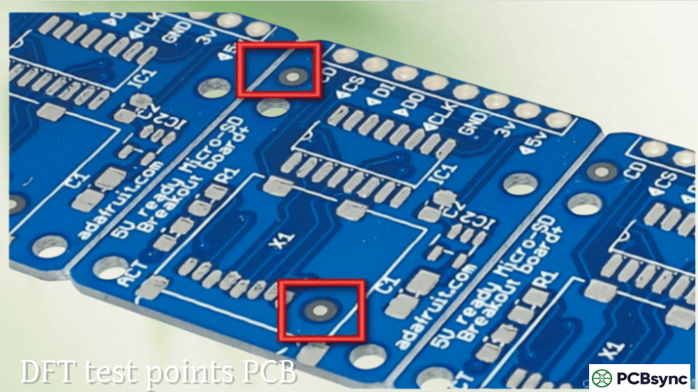
Fiducial Placement
Fiducial markers enable automated assembly equipment to precisely locate component positions. Proper fiducial placement is essential for fine-pitch component accuracy.
Global fiducials: Place at least two (preferably three) global fiducials in opposite corners of the PCB. These establish the board’s position and orientation.
Local fiducials: For fine-pitch components (≤0.5mm pitch), place local fiducials near each component—typically two fiducials within 20mm of the component.
Fiducial specifications:
Diameter: 40 mil (1mm) typical
Clearance: 100-125 mil (2.5-3mm) of bare copper around fiducial
KiCad: DRC with basic manufacturing rules, community-developed additional checks.
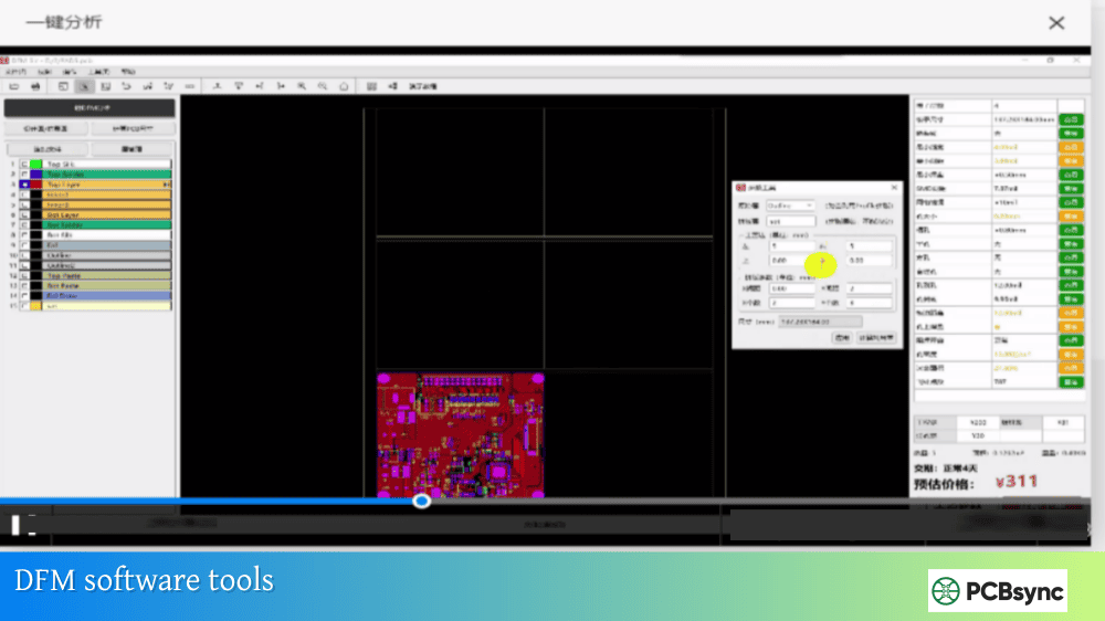
Online DFM Check Tools
Several manufacturers offer free online DFM analysis:
JLCDFM: Web-based DFM and DFA analysis tool—upload Gerbers for comprehensive manufacturability check with interactive viewer.
Sierra Circuits Better DFM: Free online tool checking annular rings, drill-to-copper clearance, and other fabrication rules.
Industry Standards References
IPC Standards for DFM:
IPC-2221: Generic Standard on Printed Board Design
IPC-2222: Sectional Standard on Rigid Organic Printed Boards
IPC-2223: Sectional Standard on Flexible Printed Boards
IPC-7351: Generic Requirements for Surface Mount Design
IPC-A-610: Acceptability of Electronic Assemblies
Manufacturer Design Guides: Most PCB fabricators publish capability documents and DFM guidelines specific to their processes. Request these documents and design to their specifications for best results.
Frequently Asked Questions About DFM PCB
What is the difference between DFM and DRC?
DRC (Design Rule Check) verifies that your design meets the rules defined in your CAD tool—rules that you set based on your requirements. DFM (Design for Manufacturing) evaluates whether your design can actually be manufactured efficiently and reliably given real-world fabrication and assembly capabilities. DRC catches violations of your specified rules; DFM catches designs that meet your rules but still cause manufacturing problems. For example, your DRC might allow 4-mil traces because your tool permits it, but DFM analysis would flag these as requiring expensive fine-line processing. Effective design requires both: DRC during layout to catch rule violations, and DFM analysis before release to verify manufacturability.
How much can DFM PCB optimization save on manufacturing costs?
Proper DFM PCB optimization typically reduces manufacturing costs by 20-40% compared to unoptimized designs. Savings come from multiple sources: optimized layer count (each layer adds 15-20% to board cost), standard via sizes (special vias add 20-50% to drilling cost), efficient panelization (20% improvement in panel utilization directly reduces per-board material cost), and higher yields (reducing scrap from 5% to 1% saves 4% on production costs plus eliminates rework). One case study showed a 15% cost reduction simply by standardizing component footprints and optimizing trace widths—changes that required no functional compromise. The savings compound in production: a $0.50 per-board savings on 10,000 boards equals $5,000 per production run.
When should I involve the PCB manufacturer in DFM review?
Involve your PCB manufacturer as early as possible—ideally during the design concept phase before layout begins. At minimum, share your preliminary design for DFM review before finalizing layout. Many manufacturers offer free DFM review services because catching issues early saves everyone time and money. Key checkpoints for manufacturer involvement: (1) before layout starts, to confirm capabilities match design requirements; (2) after initial placement and routing, to catch issues while changes are easy; (3) before final release, for comprehensive DFM verification. Building a relationship with your manufacturer creates partnership benefits: they’ll flag concerns proactively, suggest optimizations, and prioritize your jobs when capacity is tight.
What are the most common DFM errors that cause production delays?
The most common DFM errors causing delays include: insufficient annular rings (30% of DFM issues), inadequate trace-to-edge clearance (20%), missing or incorrect drill files (15%), solder mask issues (10%), and missing fiducials (10%). These errors share a common trait: they’re easily prevented with proper design rules and pre-release verification. Other frequent issues include: via-in-pad without specification of fill/cap requirements, silk screen overlapping pads, incorrect stack-up documentation, and missing impedance specifications. Most of these are caught by automated DFM tools, which is why running DFM checks before submission prevents the majority of delays. One study found that designs passing DFM review had 90% fewer engineering queries during production compared to designs released without DFM verification.
How does IPC class selection affect DFM requirements?
IPC class selection (Class 1, 2, or 3) dramatically affects DFM requirements and costs. Class 1 (consumer electronics) has the most relaxed requirements—boards must function but have the widest acceptance criteria. Class 2 (industrial/commercial) requires dedicated service reliability with tighter tolerances. Class 3 (high-reliability: medical, aerospace, military) demands the strictest manufacturing and inspection criteria with the tightest tolerances. Specifying higher classes than necessary increases costs significantly—Class 3 boards typically cost 30-50% more than Class 2 for identical designs due to tighter process controls and more rigorous inspection. Choose the class appropriate for your application: consumer products rarely need Class 3 specifications. If your application genuinely requires Class 3 reliability, design explicitly for it from the start—you can’t achieve Class 3 reliability by simply specifying it on a Class 2 design.
Useful Resources for DFM PCB Design
Industry Standards:
IPC-2221B: Generic Standard on Printed Board Design—the foundational standard for PCB design rules.
IPC-7351C: Generic Requirements for Surface Mount Design and Land Pattern Standard—component footprint specifications.
IPC-A-600: Acceptability of Printed Boards—defines fabrication quality criteria.
IPC-A-610: Acceptability of Electronic Assemblies—defines assembly quality criteria.
KiCad DRC Documentation: Design rule check setup and customization.
Manufacturer Resources:
Most PCB fabricators publish detailed DFM guidelines—request capability documents from your preferred suppliers and design to their specific processes for optimal results.
Implementing DFM PCB in Your Design Process
Effective DFM PCB isn’t a checklist you run once before manufacturing—it’s a mindset that informs decisions throughout the design process. Start by understanding your manufacturer’s capabilities before beginning layout. Set design rules that provide margin beyond minimum capabilities. Run DFM checks iteratively as the design progresses, not just at the end.
Build relationships with your manufacturers. Their engineers see thousands of designs and know exactly what causes problems. A five-minute conversation before you start can prevent a week of delays later. When they suggest changes, listen carefully—they’re trying to help you succeed.
Document everything explicitly. Ambiguity creates problems. Specify surface finishes, copper weights, impedance requirements, and tolerances clearly. Include comprehensive fabrication and assembly notes. The goal is that anyone reviewing your files knows exactly what you intend without having to ask.
Finally, learn from every production run. When issues arise, understand what caused them and update your design practices. Over time, you’ll develop intuition for what works and what causes problems—and your projects will benefit from faster manufacturing, lower costs, and higher quality.
DFM PCB practices are the difference between designs that manufacture smoothly and designs that stumble through production. The investment in learning and applying these principles pays dividends on every project you complete.
Inquire: Call 0086-755-23203480, or reach out via the form below/your sales contact to discuss our design, manufacturing, and assembly capabilities.
Quote: Email your PCB files to Sales@pcbsync.com (Preferred for large files) or submit online. We will contact you promptly. Please ensure your email is correct.
Notes: For PCB fabrication, we require PCB design file in Gerber RS-274X format (most preferred), *.PCB/DDB (Protel, inform your program version) format or *.BRD (Eagle) format. For PCB assembly, we require PCB design file in above mentioned format, drilling file and BOM. Click to download BOM template To avoid file missing, please include all files into one folder and compress it into .zip or .rar format.


