Inquire: Call 0086-755-23203480, or reach out via the form below/your sales contact to discuss our design, manufacturing, and assembly capabilities.
Quote: Email your PCB files to Sales@pcbsync.com (Preferred for large files) or submit online. We will contact you promptly. Please ensure your email is correct.
Notes: For PCB fabrication, we require PCB design file in Gerber RS-274X format (most preferred), *.PCB/DDB (Protel, inform your program version) format or *.BRD (Eagle) format. For PCB assembly, we require PCB design file in above mentioned format, drilling file and BOM. Click to download BOM template To avoid file missing, please include all files into one folder and compress it into .zip or .rar format.
PCB DFM Checklist: 25 Critical Items to Review Before Manufacturing
Every PCB engineer has been there—you submit your Gerbers confident everything looks perfect, only to get an email from your fab house flagging issues that require a respin. It’s frustrating, expensive, and entirely preventable. A solid DFM checklist PCB review catches these problems before they become costly mistakes.
After years of dealing with manufacturing delays and yield issues, I’ve compiled this comprehensive PCB DFM checklist covering 25 critical items you need to verify before sending your design to production. This isn’t theoretical stuff—these are the real checks that prevent real problems on the manufacturing floor.
Design for Manufacturability (DFM) bridges the gap between what looks good in your CAD tool and what actually works in production. Your design software doesn’t know your fabricator’s equipment limitations. It doesn’t understand that a 3-mil trace might etch inconsistently on their line, or that their drill registration has a certain tolerance that affects your annular rings.
Running through a DFM checklist PCB review before submitting files accomplishes three things: it reduces production delays, lowers per-board costs, and improves overall yield. Industry estimates suggest that 60-80% of product costs are locked in during the design phase. Catching a DFM violation now costs nothing—catching it after fabrication starts costs real money.
The Complete PCB DFM Checklist: 25 Critical Items
I’ve organized these checklist items into five categories that mirror how most DFM analysis tools structure their reviews: drill checks, signal layer checks, power/ground layer checks, solder mask checks, and silkscreen checks.
Drill Layer Checks (Items 1-7)
Drilling is the first irreversible step in PCB fabrication. Once holes are drilled, there’s no going back. These checks ensure your via and hole designs are within pcb manufacturing tolerances.
1. Minimum Drill Size Verification
Confirm your smallest drill size matches your manufacturer’s capability. Most standard fabs handle 0.2mm (8 mil) holes reliably. Going smaller (0.15mm or below) typically requires laser drilling and increases cost significantly.
Drill Type
Standard Capability
Advanced Capability
Mechanical Through-Hole
0.2mm (8 mil)
0.15mm (6 mil)
Laser Microvia
0.1mm (4 mil)
0.075mm (3 mil)
Blind/Buried Via
0.15mm (6 mil)
0.1mm (4 mil)
2. Aspect Ratio Compliance
The aspect ratio (board thickness divided by smallest drill diameter) determines plating reliability. High aspect ratios make it difficult for plating solution to reach the center of the hole barrel.
Keep aspect ratios below 10:1 for through-holes and below 0.75:1 for microvias. For a standard 1.6mm board, this means your minimum via should be at least 0.16mm. Exceeding recommended ratios risks incomplete plating and intermittent connections.
3. Drill-to-Copper Clearance
This is the distance between the drilled hole edge and the nearest copper feature. Insufficient clearance causes shorts when drill registration shifts during fabrication.
Maintain minimum 8 mils (0.2mm) drill-to-copper clearance. Account for the fact that the finished hole will be smaller than the drilled hole due to copper plating (typically 0.5-1 mil per side).
4. Annular Ring Width
The annular ring is the copper pad area surrounding a plated hole. It’s critical for electrical connection reliability between traces and vias.
IPC Class
External Layers
Internal Layers
Class 1
1 mil minimum
0 mil (tangency allowed)
Class 2
2 mil minimum
1 mil minimum
Class 3
3 mil minimum
2 mil minimum
For most commercial applications (Class 2), target 5-6 mils annular ring to provide adequate margin for drill registration tolerance. This prevents tangency (hole touching pad edge) and breakout (hole extending beyond pad).
5. Via-in-Pad Specification
If your design uses via-in-pad for BGA escape routing or thermal management, specify the fill and planarization requirements clearly. Unfilled vias under component pads cause solder wicking during reflow, starving the pad of solder.
Options include conductive epoxy fill, non-conductive fill with copper cap, or copper-filled vias. Each has different cost and performance implications—confirm your fabricator supports your chosen method.
6. Drill File Completeness
Verify your drill files include all hole types with correct tool assignments. Common mistakes include missing non-plated holes (NPTH) or failing to separate plated from non-plated drill files.
Your drill package should contain separate files for plated through-holes, non-plated holes, and any blind/buried via layers. Include a drill chart specifying hole sizes, quantities, and plating requirements.
7. Hole-to-Hole Spacing
Minimum spacing between adjacent holes prevents drill breakout and structural weakness. Standard minimum is 10 mils (0.25mm) edge-to-edge between plated holes.
For non-plated holes near plated holes, increase this to 12-15 mils to account for potential drill wandering.
Signal and Mixed Layer Checks (Items 8-13)
These checks apply to your copper routing layers where traces carry signals and power.
8. Minimum Trace Width
Trace width affects current capacity, impedance, and manufacturability. Narrower traces are harder to etch consistently and more susceptible to open circuits from minor defects.
Copper Weight
Standard Minimum
Advanced Minimum
0.5 oz
3 mil (0.075mm)
2.5 mil
1 oz
4 mil (0.1mm)
3 mil
2 oz
6 mil (0.15mm)
5 mil
For reliable pcb manufacturing, stay above your fab’s stated minimum by at least 1 mil. Use the IPC-2221 formula to verify trace width meets current requirements.
9. Trace-to-Trace Spacing
Minimum spacing between adjacent traces prevents shorts and maintains signal integrity. This spacing depends on copper weight, voltage levels, and manufacturer capability.
Standard minimum is 4-5 mils for 1 oz copper. For high-voltage applications, consult IPC-2221 spacing tables based on your working voltage and pollution degree.
10. Copper-to-Board-Edge Clearance
Copper features too close to board edges risk exposure after routing. The routing process removes material, and any misalignment could expose copper traces.
Maintain minimum 10 mils (0.25mm) copper clearance from board edges. For V-scored panels, increase this to 15-20 mils since V-scoring removes more material than tab routing.
11. Acid Trap Detection
Acid traps are acute angles (less than 90°) in copper features where etching solution can pool and over-etch the trace. This creates opens or weakened connections.
Avoid angles smaller than 90° where traces meet pads or change direction. Use 45° chamfers or curved corners instead of sharp angles. Most DFM tools flag acid traps automatically.
12. Copper Sliver Detection
Slivers are narrow strips of copper (typically less than 3 mils wide) that can detach during fabrication and cause shorts elsewhere on the board.
Set minimum copper feature width to match your minimum trace width. Remove or fill isolated copper slivers that serve no electrical purpose. Pay special attention to areas around component pads and polygon pour boundaries.
13. Thermal Relief Verification
Thermal reliefs are the spoke patterns connecting pads to copper pours. They control heat flow during soldering—too much thermal connection and the pad won’t heat properly; too little and you lose thermal/electrical performance.
Check for “starved thermals” where spokes are too thin or where gaps in the pour create incomplete connections. Standard thermal spoke width is 10-12 mils with 10 mil air gaps.
Power and Ground Layer Checks (Items 14-17)
Power and ground planes have specific DFM requirements related to clearances and thermal management.
14. Plane Clearance Around Holes
Anti-pads (clearances around non-connecting holes in plane layers) must be large enough to prevent shorts when drill registration shifts.
Minimum anti-pad clearance is typically 8-10 mils larger than the drill diameter on each side. For a 0.3mm drill, your anti-pad diameter should be at least 0.7mm.
15. Plane Isolation and Splits
If your design has split planes for different voltage rails, verify adequate separation between plane sections. Narrow gaps between plane sections are difficult to etch and may create unintended connections.
Minimum plane-to-plane spacing should match your trace-to-trace spacing requirements, typically 5-8 mils.
16. Copper Balance and Thieving
Uneven copper distribution causes board warpage during lamination and can affect impedance consistency. Large areas of bare substrate next to dense copper regions are problematic.
Add copper thieving (non-functional copper patterns) in low-density areas to balance copper distribution across each layer. Target 40-60% copper coverage per layer.
17. Thermal Via Arrays
For boards with high-power components, verify thermal via arrays are properly designed to transfer heat to inner or opposite-side copper.
Thermal vias should be 0.3mm minimum diameter, placed on 1mm pitch grid, and connected to heat-spreading copper on multiple layers. Avoid vias directly under component thermal pads (use via-in-pad with fill if necessary).
Solder mask protects copper and defines solderable areas. Errors here cause assembly defects.
18. Solder Mask Expansion/Clearance
Solder mask openings must be larger than the copper pads they expose. Standard expansion is 2-3 mils per side (4-6 mils total).
Pad Type
Recommended Expansion
SMD Pads
2-3 mils per side
Through-Hole Pads
3-4 mils per side
Fine-Pitch (<0.5mm)
1.5-2 mils per side
19. Solder Mask Web (Dam) Width
The solder mask web is the mask material remaining between adjacent pad openings. It prevents solder bridging during reflow.
Minimum solder mask web width is 3-4 mils for most processes. For fine-pitch components (0.5mm pitch or less), this becomes challenging—discuss options with your fabricator before committing to a design.
20. Via Tenting Specification
Decide whether vias should be tented (covered with solder mask), plugged, or left open. This affects assembly quality and board protection.
Tent vias smaller than 0.3mm diameter to prevent solder wicking. Larger vias may need plugging. Specify your intent clearly in fabrication notes—don’t leave it to manufacturer interpretation.
21. Solder Mask-Defined vs. Non-Solder-Mask-Defined Pads
For BGAs and fine-pitch components, decide whether pads should be SMD (solder mask opening smaller than copper pad) or NSMD (solder mask opening larger than copper pad).
NSMD pads are preferred for most applications as they provide larger solderable area and better self-centering during reflow. Document your choice clearly in the fab drawing.
Silkscreen Layer Checks (Items 22-25)
Silkscreen aids assembly and debugging. Poor silkscreen design causes confusion and slows production.
22. Silkscreen-to-Pad Clearance
Silkscreen ink on solderable pads contaminates solder joints and causes reliability issues.
Maintain minimum 5 mils clearance between silkscreen elements and solder mask openings. Most CAD tools can automate this with silkscreen clipping rules.
23. Silkscreen Line Width and Text Height
Thin silkscreen lines don’t print consistently. Small text becomes illegible.
Element
Minimum Value
Recommended Value
Line Width
4 mils
5-6 mils
Text Height
25 mils
32-40 mils
Stroke Width
4 mils
5 mils
24. Reference Designator Visibility
Every component should have a visible reference designator for assembly and debugging. Designators hidden under components are useless.
Place reference designators adjacent to components, not under them. Orient text consistently (readable from one or two board edges). Verify designators aren’t clipped by board edges or other silkscreen elements.
25. Polarity and Orientation Markings
Polarized components (diodes, electrolytic capacitors, connectors) need clear polarity indicators. Pin 1 markings on ICs should be unambiguous.
Use consistent polarity marking throughout the design (cathode bands for diodes, + symbols for capacitors). Mark pin 1 on all ICs with a dot or notch indicator. These markings dramatically reduce assembly errors.
DFM Checklist Summary Table
Here’s a quick-reference table consolidating the key parameters:
Category
Check Item
Typical Minimum
Recommended
Drill
Minimum hole size
0.2mm
0.25mm
Drill
Aspect ratio
10:1
8:1
Drill
Annular ring
2 mil (Class 2)
5-6 mil
Drill
Drill-to-copper
6 mil
8 mil
Signal
Trace width
4 mil
5 mil
Signal
Trace spacing
4 mil
5 mil
Signal
Edge clearance
10 mil
15 mil
Mask
Mask expansion
2 mil
3 mil
Mask
Web width
3 mil
4 mil
Silkscreen
Line width
4 mil
5 mil
Silkscreen
Text height
25 mil
32 mil
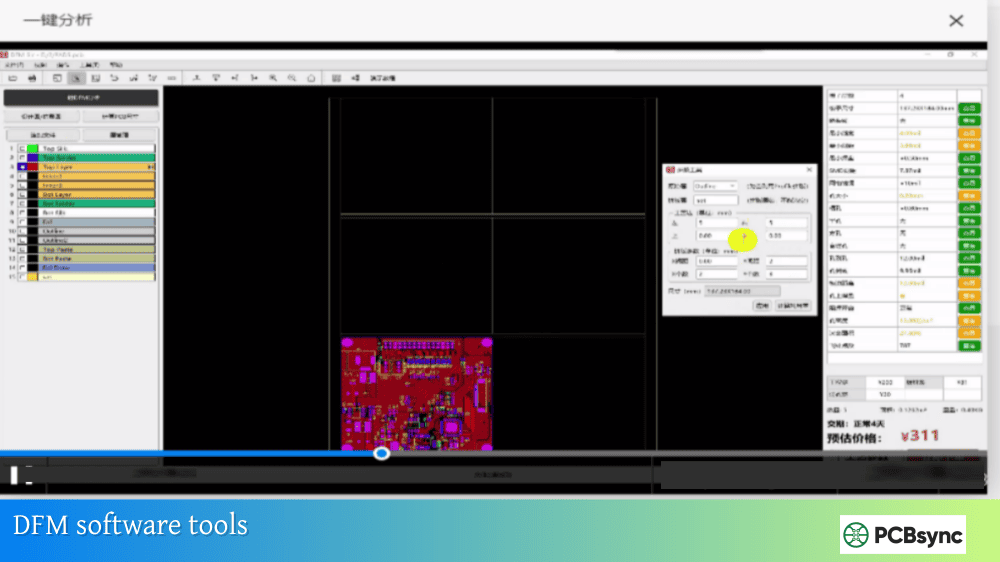
Useful DFM Resources and Tools
Here are resources that can help you implement DFM checks effectively:
Don’t wait until the end of your design to run DFM analysis. Effective DFM checklist PCB validation happens at multiple stages:
During component selection: Verify footprints match manufacturer capabilities. Check if fine-pitch parts require special processes your fab supports.
During floorplanning: Confirm layer count, stackup, and via strategy align with target manufacturer. This is when fundamental decisions get locked in.
After initial routing: Run a quick DFM check to catch obvious violations before investing more time in design refinement.
Before Gerber generation: This is your final DFM gate. Run comprehensive checks against your specific manufacturer’s capability matrix.
After Gerber export: Verify your output files in a Gerber viewer or CAM tool. Sometimes export settings cause unexpected changes.
Frequently Asked Questions
What is the difference between DFM and DRC in PCB design?
DRC (Design Rule Check) verifies your design against rules you’ve set in your CAD tool—it checks internal consistency. DFM (Design for Manufacturability) checks whether your design can actually be fabricated by a real manufacturer with real equipment tolerances. A design can pass DRC and still have DFM issues if the DRC rules don’t match the manufacturer’s capabilities.
How often should I update my PCB DFM checklist?
Review your checklist quarterly or whenever you change manufacturers. Fab capabilities evolve—what was “advanced” two years ago may be standard now. Also update after any production issue; if a defect makes it through your checklist, add a check to catch it next time.
Should I rely on my manufacturer’s free DFM check?
Manufacturer DFM checks are valuable but shouldn’t be your only line of defense. They catch issues before production, but by then you’ve already invested time finalizing your design. Running your own DFM checks during design lets you make changes when they’re cheap and easy.
What are the most commonly missed DFM items?
In my experience: insufficient annular rings, acid traps, silkscreen overlapping pads, and missing drill files for non-plated holes. Annular ring issues are particularly common because designers forget to account for drill registration tolerance.
How do DFM requirements change for HDI PCBs?
HDI boards have tighter tolerances across the board: smaller vias (0.1mm or less), finer traces (2-3 mils), and tighter spacing. Annular ring requirements become more critical because there’s less margin for error. Via-in-pad is often mandatory for BGA escape. Always confirm your fab supports HDI processes before designing to those specs.
Final Thoughts
A thorough DFM checklist PCB review isn’t optional—it’s essential. The 25 items covered here represent the checks that matter most for preventing manufacturing problems. Some will be more relevant to your specific designs than others, but understanding all of them makes you a better PCB engineer.
The best approach is building DFM thinking into your design process from the start, not bolting it on at the end. Know your manufacturer’s capabilities before you start routing. Set up your CAD tool’s design rules to match those capabilities. Run DFM checks iteratively, not just once at the end.
Your future self—the one not dealing with manufacturing delays and yield issues—will thank you.
Meta Description Suggestion:
PCB DFM Checklist: 25 critical items to verify before manufacturing. Covers drill checks, trace rules, solder mask, and silkscreen. Free downloadable checklist and DFM tool recommendations from a PCB engineer.
Inquire: Call 0086-755-23203480, or reach out via the form below/your sales contact to discuss our design, manufacturing, and assembly capabilities.
Quote: Email your PCB files to Sales@pcbsync.com (Preferred for large files) or submit online. We will contact you promptly. Please ensure your email is correct.
Notes: For PCB fabrication, we require PCB design file in Gerber RS-274X format (most preferred), *.PCB/DDB (Protel, inform your program version) format or *.BRD (Eagle) format. For PCB assembly, we require PCB design file in above mentioned format, drilling file and BOM. Click to download BOM template To avoid file missing, please include all files into one folder and compress it into .zip or .rar format.


