Inquire: Call 0086-755-23203480, or reach out via the form below/your sales contact to discuss our design, manufacturing, and assembly capabilities.
Quote: Email your PCB files to Sales@pcbsync.com (Preferred for large files) or submit online. We will contact you promptly. Please ensure your email is correct.
Notes: For PCB fabrication, we require PCB design file in Gerber RS-274X format (most preferred), *.PCB/DDB (Protel, inform your program version) format or *.BRD (Eagle) format. For PCB assembly, we require PCB design file in above mentioned format, drilling file and BOM. Click to download BOM template To avoid file missing, please include all files into one folder and compress it into .zip or .rar format.
After managing dozens of PCB assembly lines over fifteen years, I’ve seen the same pattern repeatedly: designs that look perfect on screen become nightmares on the production floor. Components too close for pick-and-place nozzles, missing fiducials that stop automated lines, thermal imbalances that cause tombstoning—these issues add weeks to schedules and thousands to budgets. DFA PCB principles exist precisely to prevent these problems by considering assembly requirements during design, not after boards arrive at the factory.
This guide covers the essential DFA PCB practices that separate designs flowing smoothly through production from those requiring constant intervention, rework, and delays.
DFA PCB—Design for Assembly applied to printed circuit boards—is the methodology of optimizing your board design for efficient, error-free component placement and soldering. While DFM (Design for Manufacturing) focuses on bare board fabrication, DFA addresses what happens next: mounting components onto that board reliably and cost-effectively.
The distinction matters because assembly typically costs more than fabrication. Every component must be picked, placed, and soldered—processes involving expensive automated equipment, precise thermal profiles, and multiple inspection steps. Design decisions made months earlier directly impact whether these processes run smoothly or require constant adjustment.
The Assembly Cost Impact
Assembly costs often exceed bare board fabrication costs, especially for complex designs. DFA PCB optimization directly reduces these costs:
Assembly Factor
Poor DFA Impact
Good DFA Impact
Pick-and-place efficiency
Multiple setup changes, slow cycle times
Optimized feeder arrangement, fast throughput
Reflow yield
Tombstoning, bridging, rework required
First-pass yields >99%
Inspection time
Extended AOI/X-ray, manual verification
Quick automated inspection
Rework rate
5-15% boards require touch-up
<1% rework needed
Total assembly cost
Baseline
20-35% reduction
Studies consistently show that assembly errors can increase production costs by 25-30% when not addressed during design. Fixing issues in layout costs pennies; fixing them in production costs dollars.
DFA vs. DFM: Understanding the Difference
DFM and DFA are complementary but distinct:
DFM (Design for Manufacturing): Focuses on bare board fabrication—trace widths, via sizes, copper clearances, material selection. Ensures the PCB can be reliably produced.
DFA (Design for Assembly): Focuses on component mounting—placement spacing, orientation, fiducials, soldering considerations. Ensures components can be reliably attached.
Together, they form DFX (Design for Excellence), the comprehensive approach to producible electronics. Both are essential; neither alone is sufficient.
Core DFA PCB Principles
Effective DFA PCB implementation rests on understanding automated assembly processes and designing to support them.
Optimize for Automated Assembly
Modern PCB assembly relies on automated pick-and-place machines that can place thousands of components per hour with micron-level accuracy. These machines have specific requirements that designs must accommodate:
Machine capabilities to consider:
Nozzle clearance for component pickup
Vision system requirements for alignment
Feeder compatibility for component packaging
Placement head rotation capabilities
Conveyor width limitations
Designs that ignore these capabilities force manual intervention, slower cycle times, or even inability to assemble automatically.
Minimize Assembly Steps
Every additional assembly step adds cost and opportunity for error. DFA PCB practices reduce steps by:
Eliminating components that require manual insertion
Reducing unique component types to simplify feeder setup
Standardizing on common package sizes
A board with 200 components in 15 unique package types assembles faster than one with 150 components in 40 unique packages—the setup time difference dominates.
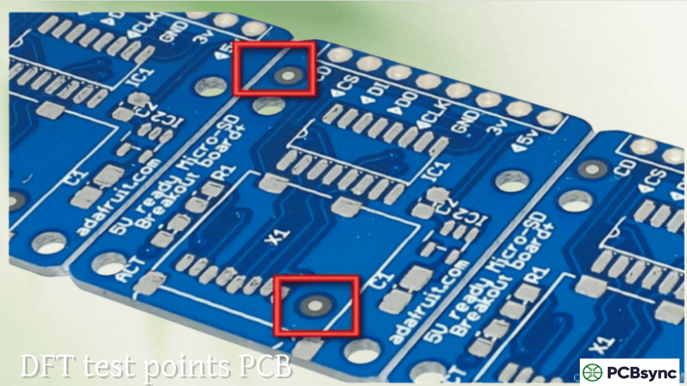
Design for Inspection and Test
Assembly isn’t complete until boards are verified. DFA PCB includes provisions for efficient quality control:
Critical components inspectable by X-ray for hidden joints
Clear reference designators for manual verification
Adequate spacing for probe access
Essential DFA PCB Component Placement Guidelines
Component placement is the foundation of DFA. Proper placement enables automated assembly; poor placement guarantees problems.
Component Spacing Requirements
Adequate spacing between components prevents physical interference during placement and ensures proper solder joint formation.
Spacing Type
Minimum
Recommended
Notes
SMD to SMD
0.5mm (20 mil)
1.0mm (40 mil)
Allows nozzle clearance
SMD to through-hole
1.0mm (40 mil)
1.5mm (60 mil)
Prevents wave solder interference
Component to board edge
3.0mm (120 mil)
5.0mm (200 mil)
Accounts for panel rails and handling
Tall to short component
0.5mm (20 mil)
1.0mm (40 mil)
Prevents reflow shadowing
Fine-pitch IC to passives
1.5mm (60 mil)
2.0mm (80 mil)
Allows rework access
Edge clearance is critical: Components too close to board edges risk damage during depanelization. V-scoring creates mechanical stress; tab routing requires clearance. The 5mm recommendation provides margin for panel rails required by assembly conveyors.
Component Orientation Best Practices
Consistent component orientation dramatically improves assembly efficiency and inspection accuracy.
Polarized components: Align all diodes, electrolytic capacitors, and ICs with consistent orientation—for example, all cathodes facing the same board edge, all IC pin 1 locations in the same relative position. This consistency:
Reduces pick-and-place head rotation by up to 20%
Simplifies AOI pattern matching
Makes visual inspection faster and more reliable
Reduces the probability of assembly errors
Passive components: Orient resistors and capacitors along common axes (0° or 90°) rather than arbitrary angles. The pick-and-place machine handles components more efficiently with fewer rotation requirements.
Wave soldering orientation: For through-hole components processed by wave solder, orient leads perpendicular to the wave direction to ensure proper solder flow and prevent shadowing.
Component Placement for Thermal Balance
Thermal management during reflow soldering prevents defects like tombstoning and cold joints.
Symmetric thermal connections: For small passive components (0603, 0402, 0201), ensure both pads have similar thermal mass connections. If one pad connects to a ground plane and the other to a thin trace, the plane acts as a heat sink, causing one pad to reach reflow temperature before the other—the classic tombstoning scenario.
Thermal relief patterns: Use thermal relief connections (spoke patterns) rather than solid connections when pads connect to copper planes. This allows pads to heat properly during soldering while maintaining electrical connectivity.
Heat-generating component isolation: Position power components, voltage regulators, and other heat sources away from temperature-sensitive parts. Include thermal vias under high-power components to dissipate heat to inner layers or heatsinks.
Fiducial Marks for DFA PCB Alignment
Fiducial marks are perhaps the simplest DFA PCB feature—small copper circles—yet their absence or improper placement stops automated assembly lines cold.
Understanding Fiducial Function
Fiducials serve as optical reference points for machine vision systems. Before placing any component, pick-and-place machines scan fiducials to determine exact board position and orientation, compensating for:
Board placement variation on the conveyor
Rotational offset from ideal position
PCB stretch or shrinkage from thermal processing
Panel-level distortion
Without fiducials, machines rely on board edges—a far less accurate reference that causes placement errors, especially for fine-pitch components.
Global Fiducial Placement
Global fiducials establish overall board position and orientation. Place at least three global fiducials on each board or panel:
Parameter
Specification
Reason
Minimum quantity
3 fiducials
Enables X, Y, and rotational correction plus distortion compensation
Pattern
Asymmetrical (triangular)
Prevents 180° orientation confusion
Location
Opposite corners
Maximizes measurement baseline for accuracy
Edge clearance
>3.85mm from board edge
Avoids conveyor clamp coverage
Spacing from each other
Maximum practical distance
Improves measurement accuracy
The three-point system: Two fiducials correct for translation and rotation. Three fiducials additionally compensate for non-linear board distortion (stretch, twist) that occurs during lamination and thermal processing—critical for fine-pitch component accuracy.
Local Fiducial Placement
Local fiducials provide precision alignment for fine-pitch components where global fiducials lack sufficient accuracy.
When to use local fiducials:
BGA packages with pitch ≤0.8mm
QFP packages with pitch ≤0.5mm
Any component requiring placement accuracy beyond ±50μm
Placement guidelines:
Position two local fiducials near opposite corners of the component
What is the difference between DFA and DFM in PCB design?
DFM (Design for Manufacturing) focuses on bare board fabrication—ensuring traces, vias, and copper features can be reliably produced by PCB fabricators. DFA (Design for Assembly) focuses on component mounting—ensuring parts can be efficiently placed and soldered onto the bare board. DFM gets you a manufacturable PCB; DFA gets you a manufacturable assembly. Both are essential: a perfectly fabricated board with poor component placement still fails in production. Most projects require attention to both, which is why they’re often combined as DFM/DFA or grouped under DFX (Design for Excellence). For complex projects, request both DFM and DFA reviews from your PCB manufacturing partners before committing to production.
How many fiducials does a PCB need for assembly?
A minimum of three global fiducials is recommended for any PCB undergoing automated assembly. Two fiducials enable X, Y, and rotational correction, but three fiducials additionally allow the vision system to compensate for non-linear board distortion (stretch, twist, warp) that occurs during fabrication. For fine-pitch components (BGA with ≤0.8mm pitch, QFP with ≤0.5mm pitch), add local fiducials—two per component—positioned near opposite corners of the package. Global fiducials should be placed asymmetrically (triangular pattern, not square) to prevent 180° orientation errors. Position all fiducials at least 3.85mm from board edges to avoid coverage by conveyor clamps.
What causes tombstoning during PCB assembly?
Tombstoning occurs when small passive components (resistors, capacitors in 0603 or smaller packages) stand upright during reflow soldering, with one end lifted off its pad. The root cause is unequal wetting forces: when solder melts on one pad before the other, surface tension pulls that end of the component upward faster than the opposing pad can anchor it down. Contributing factors include asymmetric pad sizes, unequal thermal connections (one pad connected to a ground plane, the other to a thin trace), uneven solder paste deposits, and non-uniform reflow heating. DFA prevention focuses on thermal symmetry: match copper connections on both pads, use thermal relief for plane connections, maintain symmetric pad geometry, and position small passives away from large thermal masses.
How close can components be placed to the PCB edge?
The recommended minimum clearance from components to board edge is 5mm (200 mil), though 3mm (120 mil) is sometimes acceptable for space-constrained designs. This clearance serves multiple purposes: panel rails (required for conveyor handling) typically extend 3-5mm onto the board area; depanelization (V-scoring or routing) creates mechanical stress that can damage nearby components or solder joints; and assembly fixtures often clamp board edges. Components closer than 3mm to edges risk damage during depanelization and may interfere with panel handling. For V-scored panels, maintain 5mm clearance from score lines. For tab-routed panels, keep 3mm from tab locations. Always confirm edge clearance requirements with your assembly partner.
Should I place components on one side or both sides of the PCB?
Single-sided placement is always preferred from a DFA perspective when board size permits. Single-sided assembly requires only one reflow pass, eliminating risks associated with the second side: heavy components falling off, thermal cycling stress on first-side joints, and additional process steps. However, component density requirements often necessitate double-sided placement. When using both sides, follow these DFA guidelines: place heavy and tall components on the primary (top) side; limit bottom-side components to lightweight SMT parts that won’t fall during second reflow; if bottom-side components must go through wave soldering, use adhesive to secure them; and consider the thermal history—bottom-side components experience two thermal cycles. Mixed SMT/through-hole assemblies add further complexity. Work with your assembler to determine the optimal component distribution for your specific design.
Useful Resources for DFA PCB Design
These resources support engineers implementing DFA practices:
Industry Standards:
IPC-2221: Generic Standard on Printed Board Design—includes component mounting area requirements.
IPC-7351: Generic Requirements for Surface Mount Design and Land Pattern Standard—defines recommended footprints and spacing.
IPC-A-610: Acceptability of Electronic Assemblies—inspection criteria for solder joints and component placement.
Cadence OrCAD/Allegro: Constraint-driven design with assembly rule verification.
KiCad: DRC with configurable assembly rules, BOM and placement file generation.
Online DFA Tools:
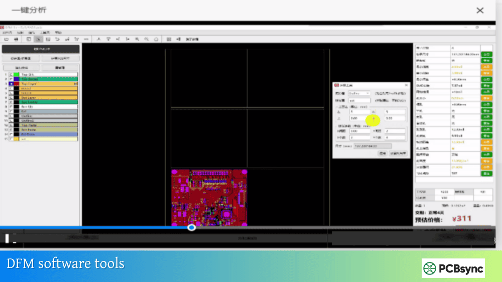
JLCDFM: Free web-based DFM/DFA analysis—upload Gerbers for comprehensive manufacturability and assembly check.
NextPCB HQDFM: Free online DFA verification tool with assembly-specific checks.
Sierra Circuits: DFA review service with engineering feedback on component placement and assembly considerations.
Assembly Partner Resources:
Most contract manufacturers publish DFA guidelines specific to their equipment and processes. Request these documents before layout begins—designing to your assembler’s capabilities prevents issues downstream.
Implementing DFA PCB in Your Design Process
Effective DFA PCB isn’t a checklist you complete at the end—it’s a mindset that influences decisions throughout design.
Start early: Consider assembly during schematic capture by selecting components with DFA-friendly packages. A through-hole connector requiring manual insertion costs more to assemble than an SMT equivalent the pick-and-place machine handles automatically.
Know your assembler: Different assembly houses have different capabilities. What one handles routinely, another may flag as problematic. Get capability documents from your intended assembler before layout, and design to their specific requirements.
Use your tools: Modern PCB design software includes DFA checking features. Enable them. Configure rules based on your assembler’s guidelines. Run checks iteratively during layout, not just at the end.
Request reviews: Before committing to production, send design files to your assembly partner for DFA review. Their engineers see thousands of designs and spot issues you might miss. This small investment of time prevents large investments in rework.
Learn from production: When assembly issues occur, investigate root causes and update your design practices. Every problem is an opportunity to improve your DFA approach for future projects.
DFA PCB practices are the difference between designs that flow through production and designs that struggle at every step. The investment in understanding assembly processes and designing to support them pays returns on every project—faster delivery, lower cost, higher quality. That’s efficient production.
Inquire: Call 0086-755-23203480, or reach out via the form below/your sales contact to discuss our design, manufacturing, and assembly capabilities.
Quote: Email your PCB files to Sales@pcbsync.com (Preferred for large files) or submit online. We will contact you promptly. Please ensure your email is correct.
Notes: For PCB fabrication, we require PCB design file in Gerber RS-274X format (most preferred), *.PCB/DDB (Protel, inform your program version) format or *.BRD (Eagle) format. For PCB assembly, we require PCB design file in above mentioned format, drilling file and BOM. Click to download BOM template To avoid file missing, please include all files into one folder and compress it into .zip or .rar format.


