Inquire: Call 0086-755-23203480, or reach out via the form below/your sales contact to discuss our design, manufacturing, and assembly capabilities.
Quote: Email your PCB files to Sales@pcbsync.com (Preferred for large files) or submit online. We will contact you promptly. Please ensure your email is correct.
Notes: For PCB fabrication, we require PCB design file in Gerber RS-274X format (most preferred), *.PCB/DDB (Protel, inform your program version) format or *.BRD (Eagle) format. For PCB assembly, we require PCB design file in above mentioned format, drilling file and BOM. Click to download BOM template To avoid file missing, please include all files into one folder and compress it into .zip or .rar format.
If you’re evaluating FPGA development boards for education, prototyping, or embedded system development, you’ve almost certainly encountered the Altera Terasic DE-series boards. Having worked with nearly every board in this lineup over the past decade, I can say that understanding the differences between models is crucial for selecting the right platform for your project.
The Terasic DE-series represents the most widely adopted family of educational FPGA boards worldwide. From the entry-level Altera DE0 to the high-performance Altera DE4, each board targets specific use cases with thoughtfully chosen peripherals and FPGA devices. This comprehensive comparison will help you navigate the options and make an informed decision.
The original Altera DE0 was designed as an affordable introduction to FPGA development. Built around the Cyclone III 3C16 device with 15,408 logic elements, it provided just enough resources for learning digital design fundamentals.
Key Features:
Cyclone III EP3C16F484C6 FPGA
346 user I/O pins
10 slide switches and 3 push buttons
4 seven-segment displays
10 green LEDs
VGA output
PS/2 connector
SD card slot
4MB Flash memory
While now phased out, many DE0 Terasic boards remain in university labs. The Cyclone III architecture, though older, still serves well for introductory courses.
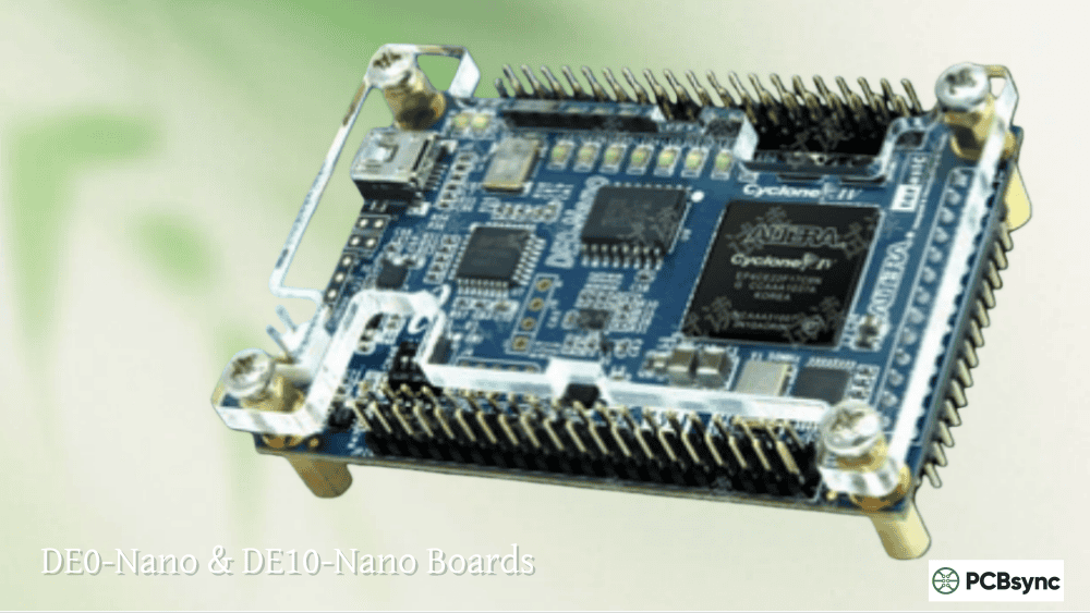
Terasic DE0-Nano
The DE0-Nano redefined compact FPGA development. Measuring just 49mm × 75mm, it packs a Cyclone IV EP4CE22 with 22,320 LEs into a credit-card-sized form factor—perfect for robotics and portable projects.
Specification
Value
FPGA Device
Cyclone IV EP4CE22F17C6
Logic Elements
22,320
Memory
32MB SDRAM, 2KB EEPROM
GPIO Headers
2 × 40-pin (72 I/O total)
LEDs
8 green
Buttons
2 momentary
Accelerometer
ADXL345 3-axis
Power Options
USB, external header, DC pins
The dual GPIO headers make the DE0-Nano incredibly versatile for interfacing with external hardware. At $108 commercial ($79 academic), it remains one of the best values in FPGA development boards.
Altera DE0-CV: The Cyclone V Upgrade
The Altera DE0-CV brings Cyclone V silicon to the entry-level segment. The DE0-CV FPGA offers 49,000 logic elements—more than double the DE0-Nano—while maintaining a compact 128mm × 99mm footprint.
DE0-CV Specifications:
Cyclone V 5CEBA4F23C7 FPGA
49,000 Logic Elements
64MB SDRAM
VGA output (4-bit per color)
PS/2 keyboard/mouse port
10 slide switches, 4 push buttons
10 red LEDs
Six 7-segment displays
2 × 40-pin GPIO headers
The DE0 CV FPGA excels for courses that have outgrown Cyclone IV boards but don’t need the complexity (or cost) of SoC-based platforms. Its VGA and PS/2 interfaces enable classic computer architecture projects.
The DE1 Series: Balanced Performance
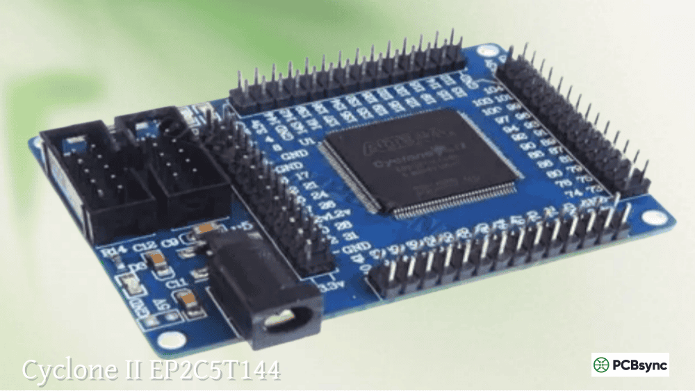
Altera DE1 (Original)
The original Altera DE1 established the template for educational FPGA boards. Based on the Cyclone II EP2C20 with 20,060 LEs, it offered a comprehensive peripheral set that influenced all subsequent DE-series designs.
Altera DE1 Features:
Cyclone II EP2C20F484C7 FPGA
8MB SDRAM, 4MB Flash, 512KB SRAM
VGA DAC with DB15 connector
24-bit audio CODEC
RS-232, PS/2, SD card
TV decoder input
10 slide switches, 4 buttons
10 red LEDs, 8 green LEDs
Four 7-segment displays
The Terasic DE1 was my first serious FPGA board, and its build quality impressed me immediately. While now discontinued, it set expectations for what educational boards should include.
DE1-SoC: The Modern Standard
The DE1 Terasic lineup evolved into the DE1-SoC, which combines an 85K LE FPGA with a dual-core ARM Cortex-A9 processor. This Altera DE1 successor has become Intel’s recommended platform for academic courses.
Subsystem
Specification
FPGA
Cyclone V 5CSEMA5F31C6
Logic Elements
85,000
ARM Processor
Dual-core Cortex-A9 @ 925MHz
FPGA Memory
64MB SDRAM
HPS Memory
1GB DDR3
Configuration
EPCS128 serial device
Video
VGA DAC (24-bit), TV decoder
Audio
24-bit CODEC with jacks
Networking
Gigabit Ethernet
USB
2× USB 2.0 host ports
Storage
Micro SD card socket
GPIO
2 × 40-pin headers, LTC connector
At $377 commercial ($249 academic), the DE1-SoC offers exceptional value for courses covering both FPGA design and embedded Linux development. The HPS (Hard Processor System) runs Linux while the FPGA fabric handles custom accelerators—a powerful combination for teaching hardware/software co-design.
The DE2 Series: Feature-Rich Educational Platforms
Altera DE2 (Original) and DE2-70
The Altera DE2 series has been the flagship educational platform since its introduction. The original DE2 with Cyclone II EP2C35 (33,216 LEs) was followed by the Altera DE2-70 with the EP2C70 (68,416 LEs).
DE2-70 Key Specifications:
Cyclone II EP2C70F896 FPGA
68,416 Logic Elements
2 × 32MB SDRAM banks
2MB SSRAM (512K × 36)
8MB Flash
Dual TV decoders (Picture-in-Picture capability)
VGA DAC
24-bit audio CODEC
10/100 Ethernet
USB host and device
RS-232, PS/2, IrDA
SD card slot
The DE2-70 became legendary for university projects. Its dual TV decoders enabled video processing labs that weren’t possible on simpler boards. Many Terasic DE2 and DE2 Terasic boards from this era remain in active use.
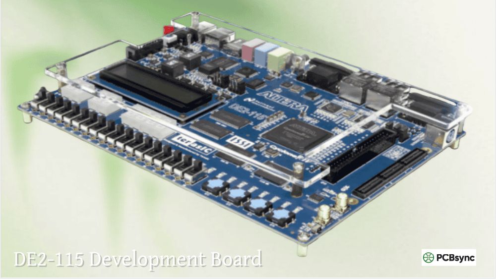
DE2-115: The Current Generation
The DE2-115 succeeded the DE2-70, upgrading to Cyclone IV EP4CE115 with 114,480 LEs—the largest device in the Cyclone IV E family. It adds dual Gigabit Ethernet and an HSMC expansion connector.
Feature
DE2-70
DE2-115
FPGA
Cyclone II 2C70
Cyclone IV 4CE115
Logic Elements
68,416
114,480
Embedded Memory
1.15 Mbit
3.89 Mbit
Multipliers
150
266
SDRAM
2 × 32MB
128MB
SRAM
2MB SSRAM
2MB
Ethernet
10/100 Mbps
2 × Gigabit
HSMC Connector
No
Yes
At $779 commercial ($423 academic), the DE2-115 remains the go-to board for advanced digital design courses requiring substantial logic resources.
High-End Research Boards: DE3 and DE4
Altera DE3: Stratix III Power
The Altera DE3 targeted ASIC prototyping and research applications requiring massive logic capacity. Based on Stratix III devices, it offered configurations from 142K to 338K logic elements.
A unique feature of the DE3 was its stackable architecture. Multiple boards could connect via HSTC (High Speed Terasic Connector) cables, creating FPGA clusters for large designs exceeding single-device capacity.
DE3 Features:
8 HSTC expansion connectors (4 male, 4 female)
2 DDR2 SO-DIMM sockets
USB host and device controllers
SD card slot
Configurable I/O voltage levels
Altera DE4: Stratix IV Performance
The Altera DE4 pushed performance further with Stratix IV GX devices featuring high-speed transceivers:
Specification
DE4-230
DE4-530
FPGA
EP4SGX230
EP4SGX530
Logic Elements
228,000
531,200
Transceivers
24 @ 8.5 Gbps
36 @ 8.5 Gbps
DDR2 Memory
2 SO-DIMM sockets
2 SO-DIMM sockets
PCIe
x8 Gen 1/Gen 2
x8 Gen 1/Gen 2
HSMC
2 connectors
2 connectors
The DE4’s PCIe connectivity made it popular for high-frequency trading accelerators and networking research. While no longer in production, these boards command premium prices on the secondary market.
The DE10 Series: Modern Successors
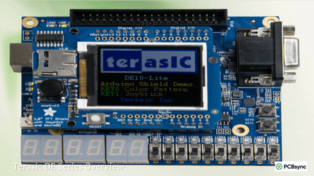
DE10-Lite: MAX 10 Introduction
The DE10-Lite brings the MAX 10 FPGA family to education at an aggressive $140 price point ($82 academic). MAX 10 devices include integrated analog-to-digital converters and instant-on configuration—no external Flash required.
The Arduino header compatibility opens access to thousands of shields, dramatically expanding the board’s capability without custom hardware development.
DE10-Nano: MiSTer Platform Standard
The DE10-Nano has achieved remarkable popularity beyond traditional FPGA development—it’s the foundation of the MiSTer retro gaming project. The board combines Cyclone V SoC capabilities with a compact form factor.
DE10-Nano Features:
Cyclone V SE 5CSEBA6U23I7 SoC FPGA
110,000 Logic Elements
Dual-core ARM Cortex-A9 @ 800MHz
1GB DDR3 (HPS)
HDMI TX output
Gigabit Ethernet
USB OTG
Micro SD card
Arduino Uno R3 header
2 × 40-pin GPIO headers
ADC (SPI interface)
At $225 ($190 academic), the DE10-Nano offers the best price-to-performance ratio for SoC development. The MiSTer community has produced hundreds of accurate recreations of classic computers and game consoles, showcasing the hardware’s capabilities.
DE10-Standard: Enhanced DE1-SoC Successor
For those needing more resources than the DE1-SoC, the DE10-Standard provides a larger FPGA (110K LEs), more memory, and an HSMC connector—all for $499.
The Terasic SoCKit deserves special mention as a collaboration between Terasic and Arrow Electronics. This SoCKit Terasic board targets developers wanting maximum Cyclone V SoC capability.
SoCKit Specifications:
Feature
Specification
SoC Device
Cyclone V SX 5CSXFC6D6F31
Logic Elements
110,000
ARM Processor
Dual-core Cortex-A9
HPS DDR3
1GB
FPGA DDR3
1GB
QSPI Flash
128MB
Transceivers
6 @ 3.125 Gbps
HSMC
With transceiver support
Audio CODEC
24-bit
VGA Output
Yes
USB OTG
Yes
Ethernet
Gigabit
The Terasic SoCKit unique feature is its high-speed transceiver access via HSMC, enabling custom high-speed interface development. While phased out, it remains popular for MiSTer ports and advanced SoC projects.
Choosing the Right Board for Your Application
For Digital Logic Courses (Beginners)
Recommended: DE10-Lite ($140/$82)
The MAX 10’s instant-on configuration and integrated ADC simplify first FPGA experiences. Students can program, see results immediately, and explore analog interfacing without external components.
Alternative: DE0-CV ($150/$95)
If your curriculum requires Cyclone V specifically, the Altera DE0-CV provides modern silicon at entry-level pricing with VGA output for graphics projects.
For Computer Architecture/Organization
Recommended: DE1-SoC ($377/$249)
The ARM+FPGA combination enables complete computer system education—from RTL design to operating system concepts. Intel’s University Program provides extensive curriculum materials specifically for this board.
Budget Alternative: DE10-Nano ($225/$190)
Same SoC architecture as DE1-SoC with fewer peripherals but better price. The compact form factor suits robotics integration.
For Advanced Design Projects
Recommended: DE2-115 ($779/$423)
When projects require maximum Cyclone IV resources, dual Gigabit Ethernet, or extensive I/O, the DE2-115 delivers. The HSMC connector enables expansion with Terasic daughter cards.
For Embedded Linux/SoC Development
Recommended: DE10-Nano ($225/$190)
Best combination of SoC capability, price, and community support. The MiSTer project demonstrates what’s achievable with this hardware.
Premium Option: DE10-Standard ($499)
Larger FPGA, HSMC expansion, and enhanced peripherals for demanding applications.
For Research/Prototyping
For high-end work, current options include:
DE10-Pro (Stratix 10)
DE10-Agilex (Agilex FPGA)
DE5a-Net-DDR4 (Arria 10)
These boards exceed $1,000 but provide cutting-edge silicon for serious research.
For absolute beginners, the DE10-Lite ($140/$82) offers the best combination of simplicity, features, and price. The MAX 10 FPGA’s instant-on capability eliminates configuration complexity, and the Arduino header provides familiar expansion options. If your institution requires Cyclone V exposure, the Altera DE0-CV is the entry-level choice in that family.
Can I run Linux on Terasic DE-series boards?
Only SoC-based boards with ARM processors support Linux: DE1-SoC, DE10-Nano, DE10-Standard, and the Terasic SoCKit. Pure FPGA boards (DE0, DE2-115, DE10-Lite) cannot run Linux directly, though you can implement Nios II soft processors that run RTOS or μCLinux with limitations.
What’s the difference between DE1-SoC and DE10-Nano?
Both use Cyclone V SoC devices with dual ARM Cortex-A9 processors. The DE1-SoC ($377) provides more peripherals (VGA, audio CODEC, TV decoder, more switches/LEDs), while the DE10-Nano ($225) offers a larger FPGA (110K vs 85K LEs), HDMI output, and compact form factor. Choose DE1-SoC for comprehensive lab exercises; DE10-Nano for embedded/portable applications.
Are older boards like the DE2-70 still worth buying?
The Altera DE2-70 and similar Cyclone II boards remain functional for learning fundamentals. However, Quartus support ended at version 13.0 SP1, meaning you cannot use modern tools or IP cores. For new purchases, invest in current-generation boards. For existing inventory, they still serve well for basic digital logic courses.
What is the MiSTer project and why does it use DE10-Nano?
MiSTer is an open-source project that accurately recreates vintage computers, consoles, and arcade machines using FPGA technology. The DE10-Nano was chosen for its combination of sufficient FPGA resources (110K LEs), ARM processor for software support, HDMI output, low cost, and availability. The community has developed cores for systems ranging from the Commodore 64 to PlayStation 1.
Power Consumption and Thermal Considerations
When designing systems around Terasic boards, understanding power requirements is essential for reliable operation.
Power Supply Requirements by Board
Board
Input Voltage
Typical Current
Power Connector
DE0-Nano
5V (USB)
200-400 mA
Mini USB / Header
Altera DE0-CV
12V DC
500-800 mA
Barrel jack
DE1-SoC
12V DC
1.5-2.0 A
Barrel jack
DE2-115
12V DC
1.5-2.5 A
Barrel jack
DE10-Lite
5V (USB)
300-500 mA
Mini USB
DE10-Nano
5V DC
1.0-2.0 A
Barrel jack
Terasic SoCKit
12V DC
2.0-3.0 A
Barrel jack
For battery-powered applications, the DE0-Nano and DE10-Lite are the most practical choices due to their USB power compatibility and lower consumption. The SoC-based boards require more substantial power supplies, especially when running Linux with active peripherals.
Thermal Management
Most Terasic boards operate without active cooling under normal conditions. However, certain scenarios require attention:
High utilization designs (>70% logic usage): Consider airflow
Hot environments (>35°C ambient): Monitor FPGA temperature
The DE10-Nano’s compact size makes heat management more critical than larger boards. For MiSTer builds running demanding cores, many users add small heatsinks or fan-equipped cases.
Expansion and Daughter Card Ecosystem
One of Terasic’s strengths is their extensive daughter card ecosystem, enabling boards to grow with project requirements.
Common Expansion Interfaces
Interface
Found On
Capabilities
GPIO (40-pin)
All boards
General I/O, 3.3V
HSMC
DE2-115, SoCKit, DE10-Standard
High-speed, transceivers
Arduino R3
DE10-Lite, DE10-Nano
Shield compatibility
LTC
DE1-SoC, DE10-Nano
SPI/I2C peripherals
Popular Daughter Cards
For Camera/Vision Projects:
TRDB-D5M: 5MP digital camera
TRDB-LTM: LCD touch panel
TRDB-DC2: Dual camera module
For Communication:
THDB-ETH: Additional Ethernet ports
THDB-SFP+: Fiber optic interface
THDB-USB: USB expansion
For Analog/Mixed Signal:
THDB-ADA: High-speed ADC/DAC
THDB-SIG: Signal conditioning
THDB-SAE: Automotive interfaces (CAN, LIN)
The HSMC ecosystem is particularly rich, allowing DE2-115, SoCKit, and DE10-Standard users to add sophisticated I/O without custom hardware development.
Software Development Workflow
Quartus Prime Workflow
All Terasic boards follow a similar development flow:
Create Project: Select target device matching your board
Design Entry: Write HDL (Verilog/VHDL) or use schematic capture
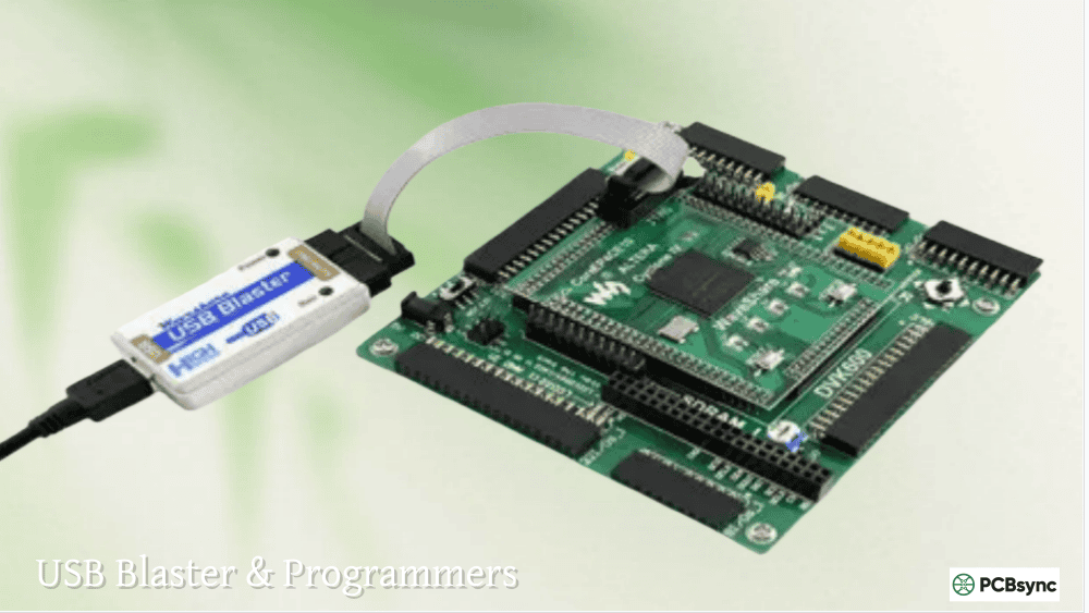
Pin Assignment: Import board-specific QSF file from Terasic
Terasic provides comprehensive support packages for each board:
System CD/Download: Documentation, schematics, examples
Control Panel: GUI for testing board peripherals
System Builder: Generates Quartus project templates
Reference Designs: Working examples for all interfaces
Always download the latest support package from Terasic’s website, as CD contents may be outdated.
Nios II Development
For soft-processor development on Altera DE2, DE0-CV, and similar boards:
Use Platform Designer (Qsys) to create system
Add Nios II processor core
Include memory controllers (SDRAM, SRAM)
Add peripherals (UART, GPIO, timers)
Generate system
Compile in Quartus
Develop software in Nios II EDS (Eclipse-based)
The Intel FPGA Monitor Program simplifies debugging by providing download, execution control, and memory inspection capabilities.
Conclusion
The Altera Terasic DE-series has shaped FPGA education for nearly two decades. From the original Altera DE0 to today’s DE10-Nano, each generation has balanced capability, cost, and educational value.
For most educational applications, I recommend starting with the DE10-Lite for pure FPGA courses or the DE10-Nano for SoC-based curricula. These boards offer modern silicon, active support, and communities that will help you succeed. The DE1-SoC remains Intel’s recommended platform for comprehensive digital design education, while the DE2-115 serves advanced projects requiring maximum Cyclone IV resources.
Whatever your needs—whether learning digital logic fundamentals, exploring embedded Linux, or prototyping custom accelerators—there’s a Terasic board designed for your application. The DE-series’ continued evolution ensures these platforms will remain relevant for years to come.
Suggested Meta Descriptions:
Option 1 (158 characters): “Complete comparison of Terasic FPGA boards: DE0, DE0-CV, DE1-SoC, DE2-115, DE10-Nano, and SoCKit. Specifications, pricing, and recommendations for each use case.”
Inquire: Call 0086-755-23203480, or reach out via the form below/your sales contact to discuss our design, manufacturing, and assembly capabilities.
Quote: Email your PCB files to Sales@pcbsync.com (Preferred for large files) or submit online. We will contact you promptly. Please ensure your email is correct.
Notes: For PCB fabrication, we require PCB design file in Gerber RS-274X format (most preferred), *.PCB/DDB (Protel, inform your program version) format or *.BRD (Eagle) format. For PCB assembly, we require PCB design file in above mentioned format, drilling file and BOM. Click to download BOM template To avoid file missing, please include all files into one folder and compress it into .zip or .rar format.


