Inquire: Call 0086-755-23203480, or reach out via the form below/your sales contact to discuss our design, manufacturing, and assembly capabilities.
Quote: Email your PCB files to Sales@pcbsync.com (Preferred for large files) or submit online. We will contact you promptly. Please ensure your email is correct.
Notes: For PCB fabrication, we require PCB design file in Gerber RS-274X format (most preferred), *.PCB/DDB (Protel, inform your program version) format or *.BRD (Eagle) format. For PCB assembly, we require PCB design file in above mentioned format, drilling file and BOM. Click to download BOM template To avoid file missing, please include all files into one folder and compress it into .zip or .rar format.
When you’re specifying FPGAs for high-performance applications, Intel’s Stratix and Arria families represent the pinnacle of programmable logic capability. Having worked on designs spanning from Stratix IV through the latest generations, I can tell you the choice between these families—and the specific devices within them—fundamentally shapes your project’s performance ceiling, power budget, and cost structure.
This guide provides a practical comparison of Intel’s high-performance FPGA families, covering everything from the EP4SE230F29I3N and EP4SGX70 in the Stratix IV lineup to the 5SGXEA7N2F45C2 in Stratix V, and extending through the Arria series including devices like the EP1AGX50DF780C6N, EP2AGX125EF29I5N, 5AGXMA3D4F31I3N, and the current-generation 10AX027H4F34E3SG.
Intel’s FPGA lineup (inherited from the Altera acquisition in 2015) splits into distinct performance tiers. At the top sits the Stratix family—the flagship line for applications demanding maximum logic density, transceiver speeds, and DSP capability. Below that, the Arria family offers a compelling balance of performance and power efficiency for mid-range applications.
Stratix Family Overview
The Stratix line has evolved through multiple generations:
The Arria series targets the sweet spot between cost and capability:
Generation
Process Node
Key Innovation
Status
Arria GX
90nm
First Arria with transceivers
Legacy
Arria II GX
40nm
Cost-optimized transceivers
Mature/Legacy
Arria V
28nm
Hard floating-point DSP
Mature
Arria 10
20nm
25.78 Gbps transceivers
Current
Stratix IV: The 40nm High-Performance Foundation
The Stratix IV family represents the 40nm generation of Intel’s high-performance FPGAs. Despite being a mature product line, you’ll still encounter these devices in legacy systems and applications where the cost of requalification outweighs migration benefits.
Stratix IV Device Variants
Intel designed three distinct variants for different application requirements:
The EP4SGX70 sits at the entry point of the Stratix IV GX family, offering a compelling combination of logic capacity and transceiver count:
Parameter
EP4SGX70
ALMs
29,040
Logic Elements
72,600
M9K Memory Blocks
462
M144K Memory Blocks
16
Total RAM Bits
4,713 Kb
DSP Blocks (18×18)
132
Transceivers (8.5G)
Up to 16
User I/O
Up to 372
Package Options
F780, F1152
The EP4SGX70 delivers 700+ GMACS of DSP performance, making it suitable for wireless infrastructure, video processing, and test equipment applications.
EP4SE230F29I3N Specifications
For applications requiring pure logic density without transceivers, the EP4SE230F29I3N from the Stratix IV E family provides substantial resources:
Parameter
EP4SE230
ALMs
91,200
Logic Elements
228,000
M9K Memory Blocks
1,235
M144K Memory Blocks
22
Total RAM Bits
14,625 Kb
DSP Blocks (18×18)
1,288
Transceivers
None
User I/O
Up to 744
Package
F29 (1152-pin FBGA)
The “I3” suffix indicates industrial temperature grade (-40°C to +100°C junction), critical for harsh environment deployments.
Stratix V: 28nm Performance Leadership
Stratix V brought substantial improvements over its predecessor, including Intel’s HyperFlex architecture precursor, enhanced transceivers, and significantly more on-chip memory.
Stratix V Device Variants
Variant
Focus
Transceiver Speed
Key Features
Stratix V GX
General high-speed
Up to 14.1 Gbps
Balanced capability
Stratix V GS
DSP-optimized
Up to 14.1 Gbps
More DSP blocks
Stratix V GT
Backplane/optical
Up to 28.05 Gbps
Highest transceiver speed
Stratix V E
Logic density
None
Maximum LEs
5SGXEA7N2F45C2 Specifications
The 5SGXEA7N2F45C2 represents one of the most capable devices in the Stratix V GX lineup, commonly found on development boards like the Terasic DE5-Net:
Parameter
5SGXEA7N2F45C2
ALMs
234,720
Logic Elements
622,000
M20K Memory Blocks
2,560
MLAB Memory Blocks
14,668
Total RAM Bits
57.16 Mb
Variable-Precision DSP
256
18×18 Multipliers
512
Transceivers (12.5G)
36
User I/O
Up to 840
Package
F45 (1932-pin FBGA)
PCIe Hard IP
Gen3 x8
This device powers demanding applications including 100G networking, high-frequency trading systems, and advanced radar processing.
Stratix V Architecture Advantages
Several architectural improvements distinguish Stratix V from earlier generations:
Variable-Precision DSP Blocks: Unlike the fixed 18×18 multipliers in Stratix IV, Stratix V DSP blocks support configurable precision from 9×9 to 36×36 bits, plus hardened IEEE 754 floating-point support—a first for FPGAs.
Enhanced Memory Architecture: The M20K blocks (20Kbit each) provide more efficient memory utilization than the M9K/M144K combination in Stratix IV. MLABs enable distributed memory implementation without consuming logic resources.
Improved Transceivers: With data rates up to 28.05 Gbps (GT variant) and hardened PCS for common protocols, Stratix V transceivers significantly reduce development time for high-speed serial designs.
Arria GX and Arria II: Cost-Optimized Transceivers
For applications where Stratix-level performance isn’t necessary but you still need integrated transceivers, the Arria GX and Arria II families provide excellent value.
EP1AGX50DF780C6N Specifications
The EP1AGX50DF780C6N belongs to the original Arria GX family, targeting cost-sensitive transceiver applications:
Parameter
EP1AGX50
ALMs
20,064
Logic Elements
50,160
M512 Memory Blocks
370
M4K Memory Blocks
183
M-RAM Blocks
2
Total RAM Bits
2,475 Kb
DSP Blocks
128
Transceivers
4-8 (up to 3.125 Gbps)
User I/O
Up to 514
Package
F780 (780-pin FBGA)
The “C6” speed grade offers the best performance for applications like Gigabit Ethernet, PCIe Gen1, and CPRI interfaces.
EP2AGX125EF29I5N Specifications
Moving to the 40nm generation, the EP2AGX125EF29I5N from Arria II GX provides substantially more capability:
Parameter
EP2AGX125
ALMs
49,640
Logic Elements
124,100
M9K Memory Blocks
495
Total RAM Bits
6,570 Kb
DSP Blocks (18×18)
288
Transceivers
Up to 16 (6.375 Gbps)
User I/O
Up to 452
Package
F29 (1152-pin FBGA)
The Arria II architecture introduced the Adaptive Logic Module (ALM) that would become standard across Intel’s FPGA lines, delivering significantly better logic efficiency than previous-generation architectures.
Arria II Key Applications
Arria II devices found widespread adoption in:
Wireless Infrastructure: CPRI and OBSAI interfaces for base station equipment
Broadcast Equipment: Triple-rate SDI processing
Network Processing: 10G/40G line cards
Industrial Automation: Motion control and machine vision
Arria V and Arria 10: Modern Mid-Range Performance
5AGXMA3D4F31I3N Specifications
The 5AGXMA3D4F31I3N represents Arria V’s capability for SoC applications, combining FPGA fabric with an integrated ARM processor:
Parameter
5AGXMA3D4F31I3N
ALMs
42,240
Logic Elements
110,000
M10K Memory Blocks
684
MLAB Memory Blocks
2,640
Total RAM Bits
7.38 Mb
Variable-Precision DSP
112
Transceivers
18 (10.3125 Gbps)
Hard Processor
Dual-core ARM Cortex-A9
User I/O
Up to 288
Package
F31 (896-pin FBGA)
The integrated ARM processor enables true heterogeneous computing, handling control plane functions while the FPGA fabric accelerates data plane processing.
10AX027H4F34E3SG Specifications
The 10AX027H4F34E3SG showcases Arria 10’s 20nm performance:
Parameter
10AX027H4F34E3SG
ALMs
101,620
Logic Elements
270,000
M20K Memory Blocks
1,512
Total RAM Bits
32.4 Mb
Variable-Precision DSP
1,518
Transceivers
Up to 48 (17.4 Gbps)
User I/O
Up to 384
Package
F34 (1152-pin FBGA)
Hard IP
PCIe Gen3 x8, DDR4
Arria 10 devices deliver up to 40% lower power consumption than previous-generation FPGAs while maintaining comparable or better performance—a critical advantage for power-constrained deployments.
Select Stratix-class devices when your application requires:
Maximum Logic Density: ASIC prototyping, large-scale compute accelerators, and complex system integration demand the hundreds of thousands (or millions) of logic elements only Stratix provides.
Highest Transceiver Performance: Applications like 400G Ethernet, coherent optical transport, and advanced radar require the 28+ Gbps transceivers available in Stratix GT/TX variants.
Memory-Intensive Processing: Video analytics, financial modeling, and AI inference benefit from Stratix’s massive on-chip memory capacity.
Compute Acceleration: Data center workloads including database acceleration, compression, and encryption see significant speedups from Stratix-based accelerator cards.
When to Choose Arria
Arria devices make more sense when:
Power Budget Constraints: Arria’s 40% power reduction versus previous generations enables deployment in 1U servers, embedded systems, and power-sensitive edge applications.
Cost Sensitivity: For production volumes where BOM cost matters, Arria delivers compelling price-performance ratios.
Adequate Performance: Many applications—including 100G networking, video transcoding, and industrial automation—perform excellently on Arria without requiring Stratix resources.
Form Factor Requirements: Arria-based accelerator cards fit in single PCIe slots and 1U chassis where Stratix solutions cannot.
Power and Thermal Considerations
Managing power consumption and thermal dissipation critically impacts high-performance FPGA designs.
Power Consumption Comparison
Device
Typical TDP
Idle Power
Maximum Power
EP4SGX70
~15W
~8W
~25W
EP4SE230F29I3N
~25W
~12W
~40W
5SGXEA7N2F45C2
~40W
~15W
~75W
EP2AGX125EF29I5N
~12W
~5W
~20W
Arria 10 GX 1150
~45W
~15W
~70W
Stratix 10 GX 2800
~100W
~30W
~225W
Thermal Design Guidelines
For Stratix IV and Stratix V designs:
Junction temperature limit: 100°C (commercial), 100°C (industrial)
Use the Intel Power Play Early Power Estimator
Plan for adequate airflow (typically 200+ LFM for high-power devices)
Consider vapor chamber or heat pipe heatsinks for maximum configurations
For Arria designs:
Lower thermal requirements enable passive cooling in many applications
Still budget for adequate PCB copper and thermal vias
Watch core voltage regulator efficiency at light loads
Development Tools and Software Support
All Intel high-performance FPGAs use the Quartus development environment, but version requirements differ:
FPGA Family
Minimum Quartus Version
Recommended Version
Stratix IV
Quartus II 9.1
Quartus II 13.1
Stratix V
Quartus II 12.0
Quartus Prime 17.1+
Arria GX
Quartus II 7.2
Quartus II 13.1
Arria II GX
Quartus II 9.1
Quartus II 13.1
Arria V
Quartus II 12.0
Quartus Prime 17.1+
Arria 10
Quartus Prime 15.1
Quartus Prime Pro 21.3+
Stratix 10
Quartus Prime Pro 17.0
Quartus Prime Pro 21.3+
Development Kit Availability
Device Family
Development Kit
Key Features
Stratix IV GX
DE4
PCIe, DDR2, HSMC
Stratix V GX
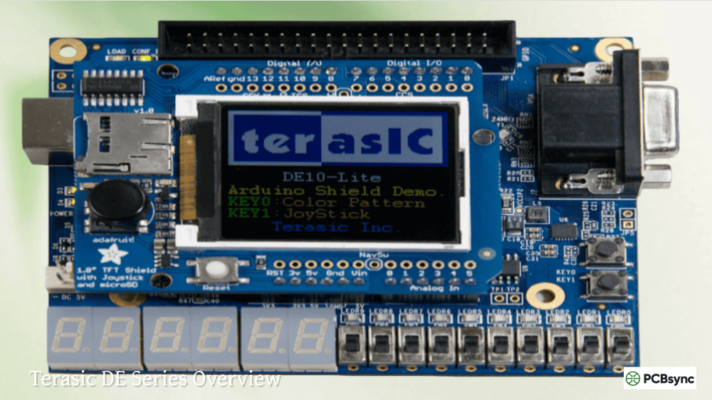
DE5-Net
PCIe Gen3, DDR3, 4×SFP+
Arria II GX
Arria II GX Dev Kit
PCIe, DDR2/DDR3, HSMC
Arria 10 GX
Arria 10 GX Dev Kit
PCIe Gen3, DDR4, QSFP+
Stratix 10
Stratix 10 GX Dev Kit
PCIe Gen3, DDR4, 100G
Migration Paths and Compatibility
Planning for device migration requires understanding pin compatibility and feature differences.
Vertical Migration Within Families
Intel supports vertical migration (moving between device densities within a package family) for most high-performance devices:
Stratix IV GX Migration: EP4SGX70 → EP4SGX110 → EP4SGX180 → EP4SGX230 (within same package)
IP core updates (some legacy IP requires replacement)
Verification regression (timing and functionality verification)
Real-World Application Examples
Data Center Acceleration
Intel’s PAC (Programmable Accelerator Card) lineup demonstrates the Stratix/Arria positioning:
Card
FPGA
Power
Memory
Target Workloads
PAC A10
Arria 10 GX
75W
8GB DDR4
Database, imaging
PAC D5005
Stratix 10 SX
215W
32GB DDR4
Analytics, video, AI
Telecommunications
Wireless Base Stations: Arria 10 devices handle CPRI/eCPRI interfaces and digital front-end processing in remote radio units where power and size constraints dominate.
Optical Transport: Stratix 10 GT devices with 58G PAM4 transceivers enable 400G coherent optical modules for long-haul networks.
Test and Measurement
Protocol analyzers and high-speed data capture systems leverage Stratix V and 5SGXEA7N2F45C2 for their combination of high-speed transceivers and substantial memory bandwidth.
What is the difference between Stratix IV GX and Stratix IV E?
Stratix IV GX devices include high-speed transceivers (up to 8.5 Gbps) for serial communication protocols, while Stratix IV E devices focus purely on logic density without integrated transceivers. Choose GX variants like the EP4SGX70 for networking and communications applications requiring SerDes interfaces. Select E variants like the EP4SE230F29I3N for ASIC prototyping or compute-intensive applications where all pins can be dedicated to parallel I/O.
Can I migrate designs from Stratix IV to Stratix V?
Direct pin-compatible migration between Stratix IV and Stratix V is not supported—the architectures differ significantly. However, Quartus provides project migration tools that handle HDL conversion and IP updates. Plan for PCB redesign, power supply modifications (different voltage requirements), and thorough verification. Most RTL code ports without major changes, though timing closure may require optimization for the new architecture.
Which Arria device should I use for 10G Ethernet applications?
For 10G Ethernet, the Arria II GX family (devices like EP2AGX125EF29I5N) provides an excellent cost-performance balance with 6.375 Gbps transceivers. For 25G or multiple 10G channels with future expansion headroom, consider Arria 10 GX devices. The 10AX027H4F34E3SG offers 17.4 Gbps transceivers with hard 10G/25G Ethernet MAC IP, simplifying implementation while reducing logic utilization.
What Quartus version supports Stratix V 5SGXEA7N2F45C2?
The 5SGXEA7N2F45C2 requires Quartus II 12.0 or later for initial support, but I recommend Quartus Prime 17.1 or newer for the best optimization results and most complete IP library. Current Quartus Prime Pro versions (21.x+) continue supporting Stratix V while providing the latest timing closure algorithms and debugging capabilities.
How do power requirements compare between Arria and Stratix families?
Power consumption differs substantially between families. Arria devices typically consume 40-70W at full utilization, fitting in 1U server slots with standard cooling. Stratix V devices like the 5SGXEA7N2F45C2 may reach 75W+ under heavy loading. Stratix 10 devices can exceed 200W, requiring 2U form factors and dedicated cooling. Always use Intel’s Power Play Estimator with your actual design—default estimates often understate real consumption for complex designs.
PCB Design Considerations for High-Performance FPGAs
Designing PCBs for Stratix IV, Stratix V, and Arria devices requires careful attention to power delivery, signal integrity, and thermal management.
Power Distribution Network
High-performance Intel FPGAs require multiple voltage rails with tight regulation:
Rail
Stratix IV
Stratix V
Arria 10
Purpose
VCCINT
0.9V
0.85V
0.9V
Core logic
VCCIO
1.2-3.3V
1.2-3.0V
1.2-3.0V
I/O banks
VCCA
2.5V
2.5V
2.5V
Analog PLLs
VCCT/VCCR
1.1V
1.1V
1.0V
Transceiver TX/RX
Design Guidelines:
Use dedicated power planes for each rail
Place bulk capacitors (100μF-470μF) near power entry points
Distribute ceramic decoupling capacitors (0.1μF, 1μF) across the device
Intel’s on-package decoupling reduces but doesn’t eliminate PCB requirements
Target PDN impedance below 5mΩ at frequencies up to 100MHz
High-Speed Signal Routing
For transceiver-equipped devices like EP4SGX70, 5SGXEA7N2F45C2, and EP2AGX125EF29I5N:
Differential Pair Requirements:
Maintain 100Ω differential impedance (±10%)
Match pair lengths within 5 mils
Route on adjacent layers when layer transitions required
Use ground-referenced stripline for best noise immunity
Avoid routing near switching power supplies or digital buses
Reference Clock Distribution:
Distribute low-jitter clocks to PLL reference inputs
Use clock buffers for fan-out rather than passive splits
Maximizing value from high-performance FPGA investments requires strategic planning.
Device Selection Guidelines
Right-Sizing Logic:
Target 70-80% utilization for production designs
Leave 20% margin for ECO fixes and feature additions
Consider slower speed grades if timing allows
Industrial grade commands 30-50% premium over commercial
Transceiver Planning:
Transceivers represent significant die area and cost
Use devices with exactly the channels needed
EP4SGX70 vs EP4SGX530: 16 vs 48 transceivers
Don’t pay for unused transceiver blocks
Development Cost Reduction
IP Core Strategy:
Leverage Intel’s free IP cores (PCIe, DDR, Ethernet)
Consider third-party IP for specialized functions
Reuse proven RTL across projects
Invest in verification IP to reduce debug time
Tool Optimization:
Use Quartus Standard Edition for cost-sensitive projects
Pro Edition required for Stratix 10 and advanced features
ModelSim-Intel FPGA Edition free for simulation
Consider DSP Builder for algorithm development
Conclusion
Selecting between Intel’s Stratix and Arria FPGA families requires balancing performance requirements against power, cost, and form factor constraints. The Stratix IV and Stratix V generations continue serving demanding applications where their combination of logic density, memory bandwidth, and transceiver capability remains unmatched in their respective technology nodes.
For new designs, Arria 10 often provides the optimal balance—delivering substantial capability at lower power and cost than Stratix alternatives. Devices like the 10AX027H4F34E3SG handle most networking, video, and industrial applications admirably. When your requirements genuinely exceed what Arria can deliver—whether in logic elements, memory capacity, or transceiver speeds—Stratix 10 awaits with the resources to match essentially any FPGA-applicable workload.
Understanding the capabilities and trade-offs of specific devices like the EP4SGX70, EP4SE230F29I3N, 5SGXEA7N2F45C2, EP1AGX50DF780C6N, EP2AGX125EF29I5N, and 5AGXMA3D4F31I3N enables informed decisions that optimize both technical performance and project economics. The key is matching device capability to actual application requirements—neither underprovisioning (leading to late-stage redesigns) nor overspecifying (wasting budget on unused resources).
Inquire: Call 0086-755-23203480, or reach out via the form below/your sales contact to discuss our design, manufacturing, and assembly capabilities.
Quote: Email your PCB files to Sales@pcbsync.com (Preferred for large files) or submit online. We will contact you promptly. Please ensure your email is correct.
Notes: For PCB fabrication, we require PCB design file in Gerber RS-274X format (most preferred), *.PCB/DDB (Protel, inform your program version) format or *.BRD (Eagle) format. For PCB assembly, we require PCB design file in above mentioned format, drilling file and BOM. Click to download BOM template To avoid file missing, please include all files into one folder and compress it into .zip or .rar format.


