Inquire: Call 0086-755-23203480, or reach out via the form below/your sales contact to discuss our design, manufacturing, and assembly capabilities.
Quote: Email your PCB files to Sales@pcbsync.com (Preferred for large files) or submit online. We will contact you promptly. Please ensure your email is correct.
Notes: For PCB fabrication, we require PCB design file in Gerber RS-274X format (most preferred), *.PCB/DDB (Protel, inform your program version) format or *.BRD (Eagle) format. For PCB assembly, we require PCB design file in above mentioned format, drilling file and BOM. Click to download BOM template To avoid file missing, please include all files into one folder and compress it into .zip or .rar format.
Choosing the right FPGA platform can make or break your design project. After spending countless hours debugging timing issues and dealing with vendor tool quirks, I’ve learned that platform selection deserves serious consideration upfront. This guide breaks down the three major FPGA Xilinx Altera players—Intel (Altera), AMD (Xilinx), and Lattice—from a practical engineering perspective.
Whether you’re prototyping with a Spartan 7 FPGA dev board, evaluating the Xilinx KCU105 for high-speed applications, or considering Lattice iCE40 UltraPlus devices for battery-powered edge computing, this comparison will help you make an informed decision.
The programmable logic market has undergone significant consolidation over the past decade. Intel acquired Altera in 2015 for $16.7 billion, while AMD completed its $50 billion acquisition of Xilinx in 2022. Lattice Semiconductor has carved out a profitable niche focusing on low-power, small form-factor devices. According to Gartner data, AMD (Xilinx) holds approximately 51% market share, Intel (Altera) commands 29%, and Lattice captures around 7%.
What does this mean for engineers? Each vendor brings distinct strengths to specific application domains. The Altera Xilinx rivalry has shaped much of FPGA architecture evolution, and understanding their different approaches helps you select the optimal platform for your requirements.
AMD FPGA Portfolio: The Xilinx Heritage
AMD’s FPGA portfolio, inherited from Xilinx, spans from cost-optimized devices to the most advanced adaptive computing platforms available. The product families follow a clear hierarchy that maps well to different project requirements.
Cost-Optimized Series: Spartan and Artix
The Spartan 7 FPGA family represents AMD’s entry-level offering, built on 28nm technology with logic densities ranging from 6K to 102K cells. These devices deliver exceptional performance-per-watt metrics, with the MicroBlaze soft processor achieving over 200 DMIPs. Key features include integrated ADC functionality, dedicated security features, and Q-grade temperature ratings (-40°C to +125°C) across all commercial devices.
From a board design perspective, Spartan-7 devices offer:
800 Mb/s DDR3 memory controller support
1.25 GB/s LVDS data rates
30% faster logic performance versus previous generations
Sub-watt power consumption in typical applications
The Artix-7 family steps up in performance while maintaining cost efficiency, making it suitable for mid-range applications requiring higher logic density and faster transceivers.
Mid-Range Performance: Kintex Series
Kintex devices occupy the sweet spot between cost and performance. The Xilinx KCU105 evaluation board, featuring the Kintex UltraScale XCKU040-2FFVA1156E FPGA, has become a standard platform for data center prototyping, wireless infrastructure development, and DSP-intensive applications.
The KCU105 includes:
DDR4 component memory interface
Eight-lane PCIe Gen3 interface
Two SFP+ connectors for 10Gbps networking
HDMI output capability
FMC HPC and LPC connectors for expansion
When I’m working on high-speed serial designs, the KCU105’s combination of GTH transceivers and comprehensive debug infrastructure significantly accelerates bring-up time.
High-Performance Computing: Virtex and Versal
For applications demanding maximum performance, AMD’s Virtex UltraScale+ devices offer HBM2 integration with up to 460 GB/s memory bandwidth. The Versal ACAP (Adaptive Compute Acceleration Platform) represents the latest evolution, combining scalar engines, adaptable engines, and intelligent engines in a heterogeneous architecture optimized for AI workloads.
SoC Integration: The FPGA ZedBoard and Zynq Family
The Zynq-7000 architecture integrates dual-core ARM Cortex-A9 processors with programmable logic, enabling hybrid hardware/software designs. The FPGA ZedBoard remains a popular development platform, featuring:
Zynq XC7Z020-CLG484 device
512 MB DDR3 memory
Gigabit Ethernet with hardware offload
HDMI, VGA, and audio interfaces
FMC expansion connector
The ZedBoard excels for Linux/Android embedded development, video processing applications, and motor control systems where real-time control loop execution benefits from dedicated hardware acceleration.
Intel Altera FPGA Architecture and Product Lines
Intel’s FPGA portfolio has evolved significantly since the Altera acquisition. The company recently spun off its Programmable Solutions Group, reestablishing Altera as an independent subsidiary while maintaining Intel’s majority ownership.
Agilex: The Next-Generation Platform
The Agilex family represents Intel’s push into heterogeneous computing, built on 10nm process technology. The architecture breaks from traditional Stratix/Arria/Cyclone naming, adopting numerical grading (3/5/7/9) that indicates performance tier:
Agilex 9: Ultra-high-end RF-grade devices with integrated high-speed AD/DA converters (up to 64 Gbps sampling), targeting defense, aerospace, and software-defined radio applications.
Agilex 7: Core high-performance lineup with 600K to 4.1M logic elements, supporting 112G PAM4 transceivers, HBM memory integration, and Network-on-Chip (NOC) architecture.
Agilex 5: Mid-range devices balancing performance with cost efficiency, featuring MIPI interfaces and industrial Ethernet support.
Agilex 3: Entry-level devices with integrated ARM Cortex-A55 dual-core HPS (Hard Processor System), offering 25K to 135K logic elements with PCIe 3.0 x4 and 10 GbE controllers.
Legacy Product Families
The Stratix, Arria, and Cyclone families continue supporting existing designs:
Stratix 10: High-end devices with Hyperflex architecture, up to 57.8 Gbps transceiver speeds, and Intel Optane persistent memory support.
Arria 10: Mid-range FPGAs and SoCs featuring ARM Cortex-A9 processor integration, suitable for video processing and 5G infrastructure.
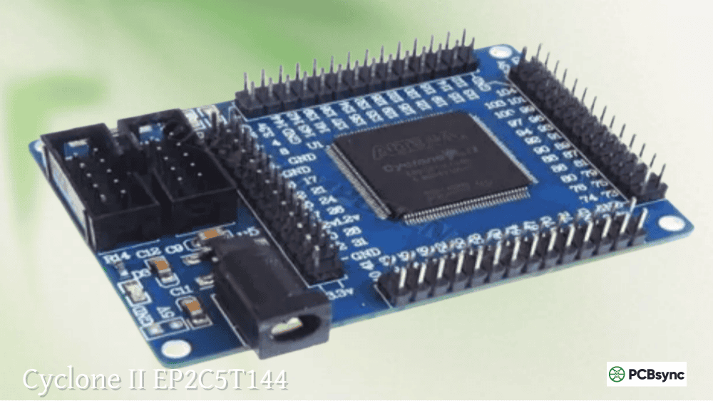
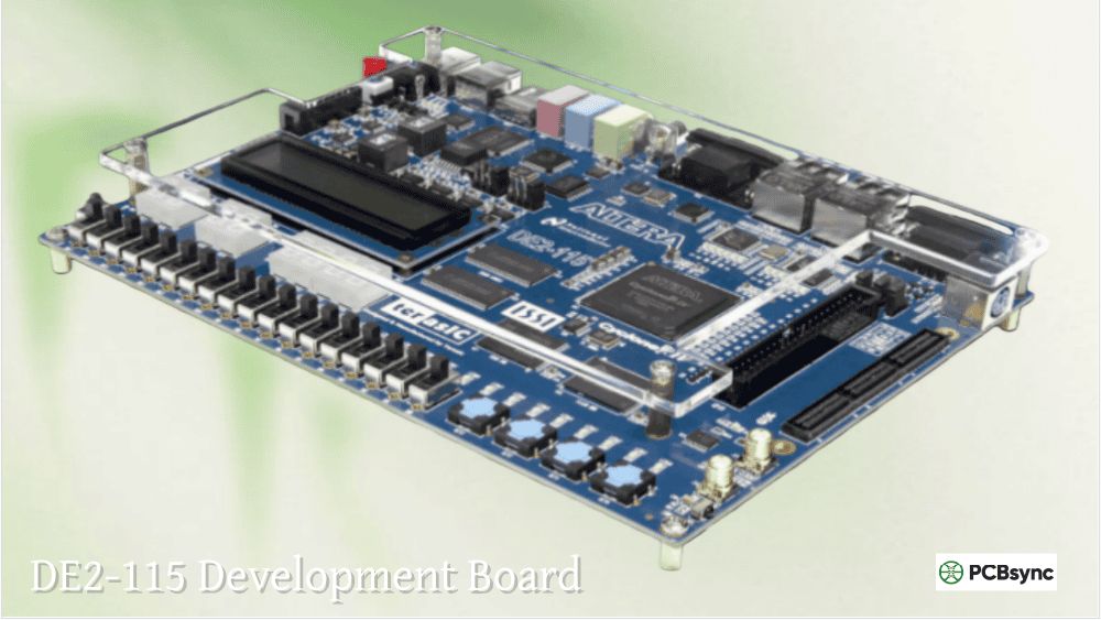
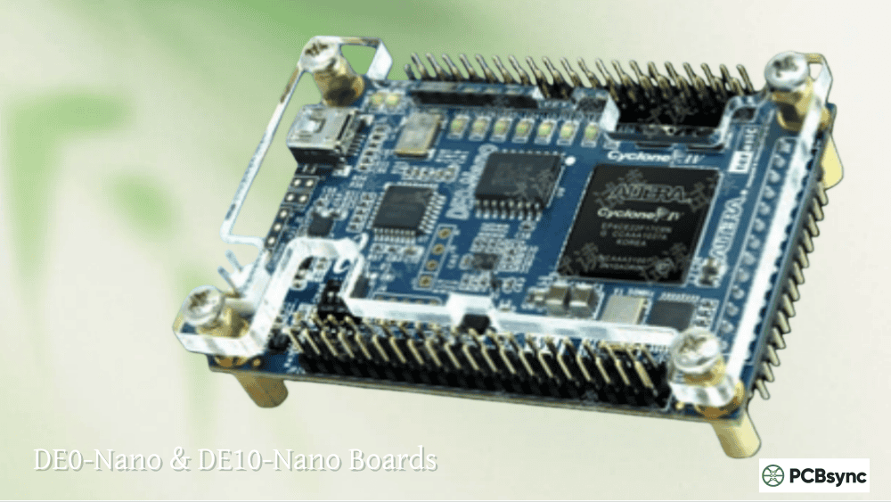
Cyclone V/10: Cost-optimized devices for high-volume applications, with the DE10-Nano being a popular development board for robotics and IoT prototyping.
MAX 10: Non-volatile FPGAs with integrated NOR flash, eliminating external configuration memory requirements—particularly useful for instant-on applications.
Design Tools: Quartus Prime
Intel’s Quartus Prime software comes in three editions:
Pro Edition: Supports Agilex, Stratix 10, Arria 10, and Cyclone 10 GX devices
Standard Edition: Covers earlier device families plus Cyclone 10 LP
Lite Edition: Free download for evaluation and high-volume device families
Lattice Semiconductor: Low-Power Leadership
Lattice has strategically positioned itself in the low-power, small form-factor segment where AMD and Intel devices are often overkill. Their FPGAs excel in applications where battery life, thermal constraints, and PCB real estate are critical design parameters.
The iCE40 Family: Ultra-Low Power Innovation
The Lattice iCE40 UltraPlus family represents the pinnacle of ultra-low power FPGA design. These devices target mobile applications, wearables, and always-on sensing applications. The ice40up architecture includes:
2800 to 5280 LUTs of programmable logic
1 Mbit single-port SRAM for data buffering
120 Kb embedded block RAM
DSP blocks for signal processing
10 kHz and 48 MHz on-chip oscillators
Package sizes as small as 2.11 mm × 2.54 mm
The FPGA Lattice iCE40 family has become extremely popular in the open-source community, partly due to Project IceStorm providing a fully open-source toolchain. This enables experimentation without vendor tool licensing constraints.
For voice recognition applications, the iCE40 UltraPlus can run always-on wake-word detection consuming mere microwatts, while higher-power application processors remain in sleep mode until triggered.
Nexus Platform: Next-Generation Low-Power
Lattice’s Nexus platform, built on Samsung’s 28nm FD-SOI (Fully Depleted Silicon-on-Insulator) process, offers:
Up to 4x lower power consumption than comparable FPGAs
I/O density twice that of similar devices
Integrated AES encryption and ECDSA authentication
Certus-NX devices with up to 40K logic cells
Avant: Entering the Mid-Range Market
The Lattice Avant platform marks the company’s expansion into mid-range FPGAs, using 16nm FinFET technology. The Avant-E series offers:
2.5x lower power consumption versus competing mid-range FPGAs
2x higher performance than previous Lattice generations
6x smaller package volume
Up to 500K logic cells
This positions Lattice to compete more directly with AMD Kintex-7 and Intel Arria families in industrial, communications, and compute applications.
FPGA Architecture Comparison: CLBs vs LABs
Understanding fundamental architecture differences helps explain performance and resource utilization variations between vendors.
AMD Xilinx Architecture
AMD uses Configurable Logic Blocks (CLBs) containing Slices. Modern 7-series and UltraScale devices feature:
Adaptive LUTs supporting various input combinations
Direct inter-LAB routing for reduced interconnect delay
Comparing resource counts between vendors is notoriously tricky since ALMs and CLBs don’t map one-to-one. Intel’s ALMs can pack more functionality per element in certain configurations, while AMD’s CLBs offer advantages in specific logic patterns.
Lattice Architecture
Lattice devices use simpler LUT4-based architectures, which trade maximum logic density for:
Lower power consumption
Faster time-to-market with simpler design flows
More predictable routing and timing closure
Development Board Comparison for Engineers
Selecting the right development board accelerates prototyping and reduces risk. Here’s a practical comparison of popular options across price points.
For engineers seeking cost-effective development platforms, Numato FPGA boards offer excellent value. The Mimas V2 features the Spartan-6 XC6SLX9 with:
512 Mb DDR SDRAM
USB 2.0 programming interface
Seven-segment display
VGA output
MicroSD card slot
At under $50, the Mimas V2 provides sufficient resources for learning FPGA design, implementing soft processors, and prototyping control systems. The Numato Narvi S7 module offers Spartan-7 capability for more demanding applications.
CPLD Considerations: The XC9500 Legacy
While FPGAs dominate complex programmable logic applications, CPLDs retain relevance for specific use cases. The XC9500 family from AMD (formerly Xilinx) represents a mature CPLD architecture offering:
Intel’s MAX V CPLDs and Lattice MachXO devices compete in this space, offering similar instant-on, non-volatile characteristics with modern I/O voltage support.
Power Supply Design Requirements by Platform
One aspect that often catches designers off-guard is the complexity of FPGA power supply design. Each vendor family has distinct power architecture requirements that significantly impact BOM cost and PCB complexity.
AMD/Xilinx Power Architecture
Modern AMD devices typically require multiple voltage rails:
VCCINT (0.85V-1.0V): Core logic supply, highest current draw
VCCAUX (1.8V): Auxiliary circuits, PLLs, JTAG
VCCBRAM (1.0V): Block RAM supply (some devices)
VCCIO (1.2V-3.3V): Bank-configurable I/O voltage
MGT supplies: Multiple rails for high-speed transceivers
For the Spartan 7 FPGA, the power architecture is relatively simple with 1.0V core and 1.8V auxiliary supplies. However, UltraScale+ devices can require 8+ separate voltage rails with strict sequencing requirements. Always consult the device power requirements early in your board design phase.
Intel/Altera Power Considerations
Intel devices follow similar multi-rail architectures:
VCCINT: Core voltage (varies by device family)
VCCIO: Per-bank I/O supplies
VCCA/VCCD: Analog and digital PLL supplies
VCCPD: Pre-driver supply for some families
The MAX 10 family simplifies this significantly with internal voltage regulators, making it attractive for space-constrained designs. Agilex devices, conversely, require sophisticated power management ICs with proper sequencing.
Lattice Power Advantages
Lattice’s FD-SOI process technology enables unique power optimization. The iCE40 UltraPlus operates from a single 1.2V or 3.3V supply with internal regulation, dramatically simplifying power design. Current consumption in standby can be under 100 µA—orders of magnitude lower than competing devices.
This power simplicity translates directly to faster design cycles and lower production costs for high-volume consumer applications.
Design Tool Ecosystem Comparison
Your development experience depends heavily on vendor tools. Here’s a practical assessment:
Aspect
AMD Vivado
Intel Quartus
Lattice Radiant
Learning Curve
Steep
Moderate
Gentle
Synthesis Speed
Moderate
Fast
Fast
GUI Usability
Improved
Traditional
Clean
Tcl Scripting
Excellent
Good
Good
HLS Support
Vitis HLS
Intel HLS
Limited
Free Tier
WebPACK
Lite Edition
Free
Linux Support
Yes
Yes
Yes
IP Catalog
Extensive
Comprehensive
Focused
High-Level Synthesis and AI Tools
Modern FPGA development increasingly leverages high-level synthesis:
AMD: Vitis unified platform, Vitis AI for machine learning
Intel: oneAPI toolkit, FPGA AI Suite, OpenCL support
Lattice: sensAI for edge ML inference, Propel for embedded design
Understanding configuration architectures helps you design reliable boot sequences and select appropriate configuration storage.
SRAM-Based FPGAs (Most AMD and Intel Devices)
Most high-density FPGAs use SRAM-based configuration cells, requiring external configuration storage:
Configuration Options:
Serial flash (SPI): Most common, cost-effective
Parallel flash (BPI): Faster boot for larger bitstreams
JTAG: Development and debugging
SD card: Convenient for prototyping
Processor-assisted: CPU loads bitstream from any storage
For the Xilinx KCU105, configuration time from QSPI flash is approximately 1.5 seconds for a full bitstream. Production designs targeting faster boot times may use parallel configuration or partial reconfiguration strategies.
Intel MAX 10: Integrated UFM (User Flash Memory) holds configuration
Lattice MachXO series: Similar flash-based architecture
XC9500 CPLDs: Non-volatile, instant-on operation
The instant-on characteristic—device operational within microseconds of power-up—is essential for power sequencing, board management controllers, and safety-critical applications.
Configuration Security
All three vendors offer bitstream encryption:
AMD: 256-bit AES with SHA-256/HMAC authentication
Intel: AES-256 encryption with design separation
Lattice: AES-128/256 with secure boot chain
For defense and high-value IP applications, evaluate each vendor’s security audit history and key management infrastructure.
Application Domain Selection Guide
Different FPGA families excel in specific application domains. This decision matrix helps narrow your selection:
Application
Recommended Vendor
Product Family
Key Advantage
Data Center Acceleration
AMD
Virtex UltraScale+
HBM integration, high LUT count
5G Infrastructure
Intel
Agilex 7
112G PAM4 transceivers
Embedded Vision
AMD
Zynq UltraScale+
ARM + GPU + FPGA integration
Battery-Powered IoT
Lattice
iCE40 UltraPlus
Microwatt-level operation
Industrial Automation
Lattice
Avant, Nexus
Low power, small packages
High-Speed Networking
Intel
Stratix 10
Transceiver performance
Consumer Electronics
AMD
Spartan-7, Artix-7
Cost optimization
Aerospace/Defense
Intel
Agilex 9
RF integration, radiation tolerance
Motor Control
AMD
Zynq-7000
Real-time processing + ARM
Prototyping
Any
Development kits
Ecosystem support
PCB Design Considerations by Vendor
As a PCB engineer, I’ve observed distinct challenges with each vendor’s device families:
AMD/Xilinx Devices
Generally require more power rails (0.9V/1.0V core, 1.8V, 3.3V auxiliary)
UltraScale+ devices need careful VCCINT power delivery design
Larger packages with higher pin counts increase routing complexity
Making Your Selection: Practical Decision Framework
After years of working across all three platforms, here’s my practical selection approach:
Define power budget first. If you’re under 100 mW total system power, start with Lattice. Their architecture is purpose-built for this constraint.
Count your logic requirements honestly. Overestimating leads to unnecessarily expensive devices. Prototype on a larger device, then migrate down.
Identify critical interfaces. High-speed transceivers, HBM, or specific ADC/DAC requirements often dictate vendor selection.
Consider ecosystem lock-in. IP investment, tool familiarity, and existing code libraries create switching costs.
Evaluate long-term availability. For production designs, verify device longevity commitments—AMD recently extended Xilinx 7-series support to 2035.
Factor in team expertise. A team experienced with Quartus will ramp faster on Intel devices, regardless of technical merits.
Frequently Asked Questions
What is the main difference between AMD FPGA and Intel FPGA architectures?
AMD (Xilinx) FPGAs use Configurable Logic Blocks (CLBs) with LUT6 architecture, while Intel (Altera) devices employ Logic Array Blocks (LABs) containing Adaptive Logic Modules (ALMs). The ALM architecture offers flexibility in how logic is packed, potentially achieving higher utilization for certain designs. AMD’s approach provides more predictable resource estimation. Both architectures deliver comparable performance for most applications, with tool quality and ecosystem support often being more significant differentiators than raw architecture.
Is Lattice iCE40 UltraPlus suitable for production designs or just prototyping?
The Lattice iCE40 UltraPlus is absolutely production-ready and actively deployed in millions of consumer devices, smartphones, and IoT products. Its ultra-low power consumption (down to 35 µA standby current) and small package options (as small as 2.11 mm × 2.54 mm) make it ideal for battery-powered production applications. Major manufacturers including LG use Lattice devices in laptop product lines. The open-source toolchain availability (Project IceStorm) is a prototyping advantage, but Lattice’s official Radiant software provides the production-grade timing analysis and synthesis optimization required for high-volume manufacturing.
Which FPGA platform offers the best value for learning and education?
For beginners, I recommend starting with either a Digilent Arty S7 board (AMD Spartan-7) around $99 or a Numato Mimas V2 (Spartan-6) under $50. Both offer sufficient resources for learning fundamentals without overwhelming complexity. If you’re on an extremely tight budget, the UPduino 3.1 with Lattice iCE40UP5K at $18 combined with the free open-source toolchain provides an excellent entry point. The FPGA ZedBoard is ideal if you want to learn both FPGA design and embedded Linux development simultaneously, though it’s pricier at around $300-500.
How do I migrate a design between AMD/Xilinx and Intel/Altera platforms?
Cross-vendor migration is possible but not trivial. RTL code (Verilog/VHDL) is generally portable, but you’ll need to address vendor-specific primitives, IP cores, and timing constraints. Key migration steps include replacing instantiated primitives (like BUFG, IBUFDS), regenerating IP blocks using the target vendor’s tools, updating constraint files (XDC to SDC format), and re-validating timing closure. Resource utilization will differ due to CLB vs ALM architectural differences. Plan for 2-4 weeks of engineering effort for moderately complex designs, longer for designs heavily dependent on vendor IP.
What’s the future outlook for CPLD devices like the XC9500 series?
Traditional CPLDs including the XC9500 family are in mature/maintenance phase, with new designs increasingly migrating to small FPGAs. However, CPLDs retain value in applications requiring instant-on operation, deterministic timing, and non-volatile configuration without external flash. Intel’s MAX V and Lattice MachXO families continue as active CPLD alternatives. For new designs, consider Lattice MachXO3 or Intel MAX 10 devices, which offer CPLD-like instant-on behavior with significantly more logic resources and modern I/O support. The XC9500 series remains available for legacy system maintenance and repair.
Conclusion
Selecting between Intel Altera, AMD Xilinx, and Lattice FPGAs requires balancing technical requirements against practical constraints. AMD/Xilinx dominates high-performance computing and data center applications with the most comprehensive product portfolio. Intel/Altera excels in high-speed communications and is pushing heterogeneous integration with Agilex. Lattice owns the low-power edge, delivering solutions impossible to match with larger FPGAs.
My recommendation: start with a clear understanding of your power budget, performance requirements, and long-term production volume. Prototype early on affordable development boards like the ZedBoard, DE10-Nano, or UPduino depending on your target segment. The right platform for your project exists—it’s just a matter of matching capabilities to requirements.
This comparison reflects market conditions and product specifications as of late 2025. FPGA families and roadmaps evolve continuously—always verify current specifications with vendor documentation before finalizing design decisions.
Inquire: Call 0086-755-23203480, or reach out via the form below/your sales contact to discuss our design, manufacturing, and assembly capabilities.
Quote: Email your PCB files to Sales@pcbsync.com (Preferred for large files) or submit online. We will contact you promptly. Please ensure your email is correct.
Notes: For PCB fabrication, we require PCB design file in Gerber RS-274X format (most preferred), *.PCB/DDB (Protel, inform your program version) format or *.BRD (Eagle) format. For PCB assembly, we require PCB design file in above mentioned format, drilling file and BOM. Click to download BOM template To avoid file missing, please include all files into one folder and compress it into .zip or .rar format.


