Inquire: Call 0086-755-23203480, or reach out via the form below/your sales contact to discuss our design, manufacturing, and assembly capabilities.
Quote: Email your PCB files to Sales@pcbsync.com (Preferred for large files) or submit online. We will contact you promptly. Please ensure your email is correct.
Notes: For PCB fabrication, we require PCB design file in Gerber RS-274X format (most preferred), *.PCB/DDB (Protel, inform your program version) format or *.BRD (Eagle) format. For PCB assembly, we require PCB design file in above mentioned format, drilling file and BOM. Click to download BOM template To avoid file missing, please include all files into one folder and compress it into .zip or .rar format.
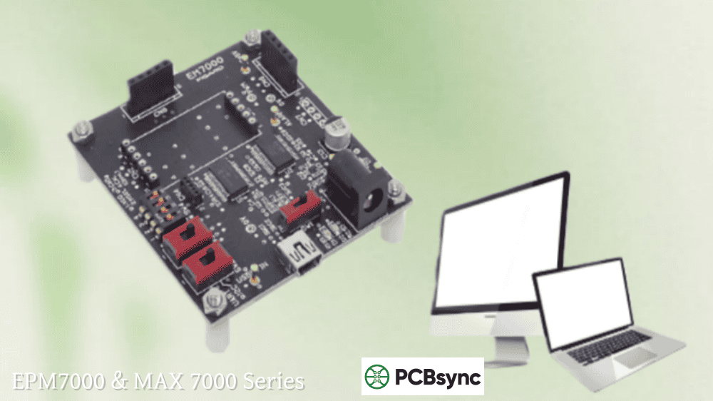
As a PCB design engineer who has worked extensively with programmable logic devices over the years, I’ve seen the Altera MAX 7000 family remain a workhorse in countless industrial and embedded applications. Whether you’re maintaining legacy equipment or prototyping new control systems, understanding devices like the EPM7128AETC100 10N, EPM7128STC100 15, and their cousins in the MAX7000A, MAX7000S, and MAX3000A families is essential knowledge.
This guide cuts through the marketing fluff and delivers practical information you actually need: pinout configurations, timing specifications, programming workflows, and real-world application guidance for the Altera CPLD and Intel CPLD device families.
The Altera MAX7000 family represents Altera’s second-generation MAX architecture, now part of Intel’s Programmable Solutions Group following the 2015 acquisition. These EEPROM-based Complex Programmable Logic Devices (CPLDs) fill the gap between simple PALs/GALs and more complex FPGAs, offering deterministic timing and non-volatile configuration storage that many engineers find invaluable.
Built on advanced CMOS EEPROM technology, the MAX 7000 family delivers 600 to 10,000 usable gates across its various subfamilies. The architecture centers around Logic Array Blocks (LABs), each containing 16 macrocells that implement custom combinational and sequential logic functions.
MAX 7000 Family Overview
The complete Altera MAX7000 ecosystem includes several subfamilies designed for different voltage requirements and feature sets:
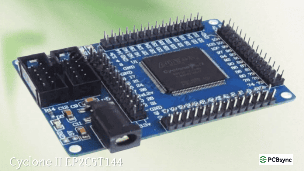
The EPM7128 has earned its reputation as the go-to device for mid-complexity designs. With 128 macrocells providing approximately 2,500 usable gates, it hits the sweet spot for control logic, state machines, and interface bridging applications.
EPM7128 Key Specifications
Parameter
EPM7128S (5V)
EPM7128A (3.3V)
Macrocells
128
128
Usable Gates
2,500
2,500
User I/O Pins
Up to 84 (100-pin package)
Up to 84 (100-pin package)
Logic Array Blocks
8 LABs
8 LABs
Max Global Clocks
2
2
Output Enables
6
6
Supply Voltage
4.75V to 5.25V
3.0V to 3.6V
Temperature Range
0°C to +70°C (commercial)
0°C to +70°C (commercial)
Popular EPM7128 Part Numbers Explained
If you’ve ever been confused by Altera’s part numbering scheme, you’re not alone. Here’s what those suffixes actually mean:
EPM7128AETC100-10N
EPM7128A: 128-macrocell MAX 7000A device
E: Extended temperature or enhanced features
TC: TQFP package type
100: 100-pin package
-10: Speed grade (10ns pin-to-pin delay)
N: Lead-free/RoHS compliant
EPM7128STC100-15
EPM7128S: 128-macrocell MAX 7000S device with ISP
TC: TQFP package
100: 100-pin package
-15: Speed grade (15ns pin-to-pin delay)
EPM7128SQC100
EPM7128S: MAX 7000S variant
QC: PQFP (Plastic Quad Flat Pack)
100: 100-pin package
EPM7128 Speed Grade Comparison
Speed grade selection significantly impacts your design’s performance ceiling. Here’s what each rating means in practical terms:
Speed Grade
Pin-to-Pin Delay
Max Internal Frequency
Best For
-5
5 ns
175.4 MHz
High-speed data paths, PCI interfaces
-6
6 ns
151.5 MHz
Fast control logic
-7
7 ns
129.9 MHz
General-purpose applications
-10
10 ns
100 MHz
Cost-sensitive designs
-15
15 ns
76.9 MHz
Low-power applications
Pinout Configuration and Package Options
Understanding pinout configurations is critical for successful PCB layout. The MAX 7000 family ships in several package formats, each with specific advantages.
The 100-pin TQFP is the most popular package for EPM7128 devices. Pin numbering follows counterclockwise convention starting from the top-left corner (pin 1 indicator dot).
Pin Distribution:
Pins 1-25: Side 1 (top edge)
Pins 26-50: Side 2 (right edge)
Pins 51-75: Side 3 (bottom edge)
Pins 76-100: Side 4 (left edge)
Critical Pin Assignments:
Function
Pin Numbers
Notes
VCC (Power)
4, 17, 30, 43, 56, 69, 82, 95
Connect all to 5V or 3.3V depending on variant
GND
11, 24, 37, 50, 63, 76, 89
Solid ground plane recommended
GCLK1
87
Global clock input 1
GCLK2
2
Global clock input 2 (MAX 7000E/S/A only)
GCLRn
1
Global clear (active low)
OE1
84
Output enable 1
OE2
2
Shared with GCLK2
TDI
14
JTAG data in (MAX 7000S/A only)
TDO
71
JTAG data out
TMS
23
JTAG mode select
TCK
62
JTAG clock
84-Pin PLCC Pinout (EPM7128SLC84)
The PLCC package remains popular for socketed applications and prototyping:
Pin Distribution:
68 User I/O pins
Standard JTAG interface on pins 14, 23, 62, 71
Power/Ground distributed evenly
Package Selection Guidelines
From my experience, here’s how I typically choose packages:
100-pin TQFP (TC): Default choice for new designs. Good I/O density, reasonable routing.
100-pin PQFP (QC): Slightly larger footprint, easier hand soldering for prototypes.
84-pin PLCC (LC): Best for development boards and socketed applications where you need to swap devices frequently.
144-pin TQFP: Required for EPM7256 and larger devices needing maximum I/O.
The EPM7032 and EPM7064 Series
For smaller designs, the EPM7032 and EPM7064 devices offer cost-effective solutions without sacrificing the MAX 7000 architecture’s benefits.
Altera EPM7032 Specifications
Parameter
EPM7032
EPM7032S
Macrocells
32
32
Usable Gates
600
600
User I/O (44-pin)
36
36
LABs
2
2
ISP Support
No
Yes
Package Options
44-pin PLCC, TQFP
44-pin PLCC, TQFP
The Altera EPM7032 fits applications where you need reliable control logic in minimal board space—think simple state machines, bus interface logic, or clock generation circuits.
EPM7064S and EPM7064SLC44 Details
The EPM7064S doubles the macrocell count over the EPM7032 while maintaining package compatibility in 44-pin versions:
Parameter
Value
Macrocells
64
Usable Gates
1,250
User I/O (68-pin)
68
User I/O (44-pin)
36
LABs
4
Max Frequency
175.4 MHz (-5 grade)
The EPM7064SLC44 variant in the 44-pin PLCC package is particularly useful when you need ISP capability in a compact, socketable form factor.
MAX 3000A Family: The Low-Cost Alternative
When budget constraints drive the design, the MAX3000A family offers similar functionality to MAX 7000A at reduced cost. These 3.3V devices use the same development tools and programming infrastructure.
MAX 3000A Device Comparison
Device
Macrocells
Gates
Max I/O
Key Package Options
EPM3032A
32
600
34
44-pin PLCC/TQFP
EPM3064A
64
1,250
66
44/100-pin TQFP
EPM3128ATC100 10N
128
2,500
80
100-pin TQFP
EPM3256ATC144
256
5,000
116
144-pin TQFP
EPM3512A
512
10,000
158
208-pin PQFP
The EPM3128ATC100 10N offers 128 macrocells in a 100-pin TQFP package with 10ns speed grade—essentially a cost-reduced alternative to the EPM7128A for designs where the MAX 3000A architecture suffices.
When to Choose MAX 3000A vs MAX 7000A
Choose MAX 3000A (EPM3064A, EPM3128ATC100 10N, EPM3256ATC144) when:
Cost is the primary driver
Design complexity is moderate
You don’t need the enhanced routing of MAX 7000A
Production volumes are high
Choose MAX 7000A when:
You need maximum speed grades (-4, -5)
Design requires complex routing
PCI compliance is mandatory
Hot-socketing support is needed (MAX 7000AE)
CPLD Architecture: Understanding the Internal Structure
To effectively use any Altera CPLD or Intel CPLD, you need to understand the internal architecture. The MAX 7000 family uses a product-term based architecture distinct from FPGA lookup tables.
Logic Array Block (LAB) Structure
Each LAB contains:
16 macrocells
36 inputs from the Programmable Interconnect Array (PIA)
Local interconnect for fast intra-LAB communication
Shared and parallel expanders for complex functions
Macrocell Architecture
The macrocell is the fundamental building block:
Components:
Product-term array (5 product terms per macrocell)
Product-term select matrix
Programmable OR gate
Programmable XOR gate
Configurable register (D, T, JK, or SR flip-flop)
Output select multiplexer
Register Modes:
Combinatorial output (bypass register)
Registered output with global clock
Registered output with array clock
Clock enable option
Programmable Interconnect Array (PIA)
The PIA serves as the central routing resource:
Connects all LABs
Receives inputs from I/O pins and macrocell feedback
Provides 36 signals to each LAB
Enables any-to-any connectivity with predictable timing
Programming Altera CPLDs with Quartus
Programming MAX 7000 devices requires the Quartus II software (legacy versions) or Quartus Prime for newer parts. Here’s the practical workflow I use.
The Altera CPLD family excels in applications requiring deterministic timing and non-volatile configuration. Here’s where I’ve deployed them successfully.
Industrial Automation
State Machine Controllers: The EPM7128S handles startup sequences, interlock logic, and error state management for industrial machinery. Its instant-on behavior ensures the control logic is active before the main processor boots.
Protocol Converters: Converting between RS-485, SPI, and parallel interfaces is straightforward with CPLDs. The deterministic timing simplifies meeting protocol specifications.
Telecommunications Equipment
Timing Generation: Global clock distribution and timing alignment for network equipment. The two global clocks and six output enables provide flexible clocking schemes.
Rate Adaptation: Data format conversion and rate matching between different interface standards.
Automotive Electronics
Engine Control Units: Glue logic between sensors, actuators, and microcontrollers. The industrial temperature range variants (-40°C to +85°C) handle harsh automotive environments.
Safety Systems: Implementing watchdog circuits and fail-safe logic that must function independently of software.
Embedded Systems
FPGA Configuration Management: CPLDs often serve as configuration controllers for FPGAs, handling power-up sequencing and configuration memory access.
Bus Interface Logic: Address decoding, chip select generation, and wait state insertion for processor buses.
Consumer Electronics
Display Controllers: LCD timing generation and interface adaptation.
Peripheral Management: Keyboard/mouse interface conversion, LED driver control.
Design Considerations and Best Practices
Power Supply Decoupling
For reliable operation, follow these decoupling guidelines:
Package Size
Capacitor Value
Placement
44-pin
0.1µF ceramic
One per VCC pin
84-pin
0.1µF ceramic
One per VCC pin, plus 10µF bulk
100-pin
0.1µF ceramic
One per VCC pin, plus 10µF bulk
144+ pin
0.1µF ceramic
One per VCC pin, plus 22µF bulk
I/O Standards and Level Shifting
MAX 7000S (5V): Native 5V TTL levels, directly interfaces with 5V logic.
MAX 7000A (3.3V) with MultiVolt I/O:
Core runs at 3.3V
I/O banks can interface with 2.5V, 3.3V, or 5V logic
5V tolerance only on input pins
Timing Closure Tips
Use Global Clocks: Route high-fanout clocks through GCLK1/GCLK2 for minimum skew
Register I/O: Use input and output registers when interfacing with external buses
Mind the Expanders: Shared and parallel expanders add delay—use sparingly in critical paths
Check Setup/Hold: Verify timing with the TimeQuest analyzer before committing to silicon
Datasheet and Resource Downloads
Here are the official sources for technical documentation:
Stock Up: Purchase lifetime buys of critical components
Document Thoroughly: Keep programming files and design archives
Test New Sources: Surplus/broker parts may have JTAG disabled or be counterfeit
Plan Migration: Develop replacement strategies for critical systems
Frequently Asked Questions
What is the difference between EPM7128S and EPM7128A?
The EPM7128S operates at 5V and belongs to the MAX 7000S family, while the EPM7128A runs at 3.3V and is part of the MAX 7000A family. Both have 128 macrocells and similar architectures, but the EPM7128A offers MultiVolt I/O capability for interfacing with multiple voltage domains. Choose EPM7128S for 5V-only systems and EPM7128A for mixed-voltage or low-power designs.
Can I program MAX 7000 CPLDs with the latest Quartus Prime?
No, MAX7000 and MAX7000A devices require Quartus II version 13.0sp1 or earlier. Intel discontinued support for these legacy devices in newer Quartus Prime versions. Download Quartus II Web Edition 13.0sp1 along with the MAX 7000 device support package from Intel’s legacy software archive.
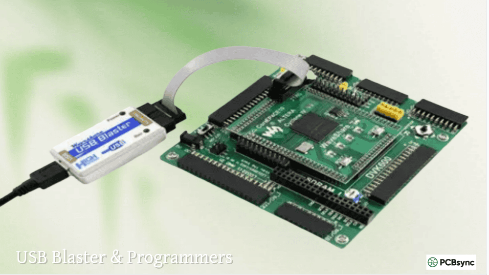
What programmer hardware do I need for EPM7128AETC100-10N?
You need a USB-Blaster or compatible JTAG programmer. The original Altera USB-Blaster, USB-Blaster II, or third-party clones (like Terasic’s version) all work. Connect the programmer to a 10-pin JTAG header on your board with TCK, TMS, TDI, TDO, VCC, and GND signals. Power the target board before attempting programming.
Are MAX 7000 CPLDs still in production?
Many MAX 7000 variants have reached end-of-life status. Intel continues to produce some MAX 7000A and MAX 3000A devices, but availability fluctuates. Check with authorized distributors (DigiKey, Mouser, Arrow) for current stock. For new designs, consider MAX II, MAX V, or MAX 10 devices which remain in active production.
How do I choose between CPLD and FPGA for my application?
Choose an Altera CPLD or Intel CPLD when you need: instant power-on operation (non-volatile configuration), deterministic timing with predictable delays, simple to moderate logic complexity (under 10,000 gates), low power consumption, or cost-sensitive high-volume production. Choose an FPGA when you require: high logic density, DSP functionality, embedded processors, high-speed serial interfaces, or dynamic reconfiguration.
Troubleshooting Common Design Issues
Over the years, I’ve encountered various issues when working with MAX 7000 devices. Here are solutions to the most common problems.
Timing Violations
Symptom: Design works in simulation but fails on hardware.
Solutions:
Check that you’re meeting setup and hold times on input pins
Verify clock frequency doesn’t exceed the device’s fMAX rating
Use registered I/O paths instead of combinatorial outputs for external interfaces
Review the timing report in TimeQuest and address any failing paths
Excessive Power Consumption
Symptom: Device runs hotter than expected or draws excessive current.
Solutions:
Enable power-saving mode on non-critical macrocells
Reduce operating frequency where possible
Check for floating inputs that cause input buffers to oscillate
Add pull-up or pull-down resistors on unused I/O pins
Consider moving to MAX 7000A (3.3V) for inherently lower power
I/O Conflicts
Symptom: Outputs don’t drive to expected levels, or contention on buses.
Solutions:
Verify output enable logic is correct for tri-state buffers
Check that OE pins are properly connected (not floating)
Ensure slew rate settings match your load requirements
Review PCB layout for signal integrity issues on long traces
Configuration Not Loading
Symptom: Device programs successfully but doesn’t function correctly.
Solutions:
Verify the correct device is selected in Quartus
Check that pin assignments match your schematic
Ensure the .pof file was fully transferred
Test with a known-good programming pattern first
Comparison: MAX 7000 vs Competing CPLD Families
Understanding how the Altera CPLD stack compares to alternatives helps inform device selection.
The MAX7000A and MAX7000S remain competitive for product-term based designs requiring predictable timing. However, for new designs where flexibility matters more than timing determinism, modern alternatives like MAX II or MAX V offer better density and lower power consumption while maintaining non-volatile configuration.
PCB Layout Guidelines for MAX 7000 Devices
Proper PCB layout is essential for reliable CPLD operation. Here are guidelines I follow on every design.
Power Distribution
Ground Plane: Always use a solid ground plane on at least one layer. The CPLD’s fast edge rates require low-impedance return paths.
Power Plane: A dedicated power plane for VCCINT significantly improves noise immunity. For smaller boards, use wide power traces instead.
Via Placement: Place vias to power and ground planes directly adjacent to each VCC and GND pin—not connected via traces.
Signal Routing
Clock Lines: Route GCLK1 and GCLK2 signals with minimum length and no layer changes. Keep these away from noisy digital signals.
JTAG Interface: The JTAG signals (TCK, TMS, TDI, TDO) should be accessible via a header for programming. Route as short, direct traces.
High-Speed Outputs: Match trace lengths for buses requiring synchronous operation. Use series termination resistors (22-33 ohms) for long traces.
Component Placement
Decoupling Capacitors: Place 0.1µF ceramics within 5mm of VCC pins. Use a larger bulk capacitor (10-22µF) near the power entry point.
Crystal/Oscillator: If using an external oscillator, place it close to the GCLK input pin with short, direct traces.
Test Points: Include test points on key signals for debugging. Access to global clock and reset lines is particularly valuable.
Conclusion
The Altera MAX 7000 family, including popular devices like the EPM7128AETC100 10N, EPM7128STC100 15, EPM7128SQC100, and their MAX3000A counterparts, continues to serve engineers well in applications demanding reliable, deterministic digital logic. While these devices represent mature technology, their straightforward architecture and non-volatile operation make them irreplaceable for many industrial, automotive, and embedded applications.
Whether you’re designing new products with the EPM7128S, EPM7064S, or EPM3128ATC100 10N, or maintaining legacy systems using the Altera EPM7032 or EPM3064A, understanding these devices’ capabilities and limitations enables you to make informed decisions that keep your projects on track and your systems running reliably.
For the latest specifications, always consult the official Intel documentation and verify part availability with authorized distributors before committing to a design.
Inquire: Call 0086-755-23203480, or reach out via the form below/your sales contact to discuss our design, manufacturing, and assembly capabilities.
Quote: Email your PCB files to Sales@pcbsync.com (Preferred for large files) or submit online. We will contact you promptly. Please ensure your email is correct.
Notes: For PCB fabrication, we require PCB design file in Gerber RS-274X format (most preferred), *.PCB/DDB (Protel, inform your program version) format or *.BRD (Eagle) format. For PCB assembly, we require PCB design file in above mentioned format, drilling file and BOM. Click to download BOM template To avoid file missing, please include all files into one folder and compress it into .zip or .rar format.


