Inquire: Call 0086-755-23203480, or reach out via the form below/your sales contact to discuss our design, manufacturing, and assembly capabilities.
Quote: Email your PCB files to Sales@pcbsync.com (Preferred for large files) or submit online. We will contact you promptly. Please ensure your email is correct.
Notes: For PCB fabrication, we require PCB design file in Gerber RS-274X format (most preferred), *.PCB/DDB (Protel, inform your program version) format or *.BRD (Eagle) format. For PCB assembly, we require PCB design file in above mentioned format, drilling file and BOM. Click to download BOM template To avoid file missing, please include all files into one folder and compress it into .zip or .rar format.
After spending fifteen years designing FPGA-based systems, I’ve programmed thousands of configuration devices—from the venerable EPC1PC8 parallel devices on legacy Flex 10K boards to modern EPCQL512 quad-serial flash on Stratix 10 designs. The EPCS serial configuration family remains the workhorse for Cyclone and older Stratix platforms, and understanding these devices thoroughly prevents countless field failures and production headaches.
This guide covers everything from basic EPCS1SI8N selection to advanced EPCS64SI16N programming techniques, drawing on real production experience and documented failure modes I’ve encountered across industrial, medical, and telecommunications applications.
Understanding EPCS Serial Configuration Device Architecture
The EPCS family represents Intel’s (formerly Altera’s) serial flash solution for storing FPGA configuration bitstreams. Unlike parallel configuration devices like the EPC1PC8 or EPC16QC100N that require multiple data pins, EPCS devices use a simple four-wire SPI interface that dramatically reduces PCB routing complexity and I/O pin consumption.
How Serial Configuration Works
When power is applied to a Cyclone or Stratix FPGA configured in Active Serial (AS) mode, the FPGA becomes the bus master. It generates the clock signal (DCLK), controls chip select (nCS), sends commands through ASDI (Active Serial Data Input), and receives configuration data on DATA0. This master-slave relationship means the FPGA controls the entire configuration sequence—a significant departure from parallel schemes where external logic or another device might drive the process.
The configuration flow proceeds as follows:
FPGA releases from reset and samples MSEL pins to determine configuration mode
FPGA asserts nCS low to select the EPCS device
FPGA sends the Read Bytes command (03h) followed by address 000000h
EPCS device streams configuration data on DATA0
FPGA latches data on DCLK rising edges until configuration completes
FPGA releases nCS and enters user mode
This entire sequence typically completes in tens of milliseconds for smaller devices like Cyclone II, extending to hundreds of milliseconds for larger configurations.
EPCS Device Family Specifications
The EPCS family spans five density options, each targeting different FPGA sizes and configuration requirements.
Complete EPCS Device Comparison
Device
Density
Sectors
Package Options
Max DCLK
Ordering Code
EPCS1
1 Mbit
4
8-pin SOIC
20 MHz
EPCS1SI8N
EPCS4
4 Mbit
8
8-pin SOIC
20 MHz
EPCS4SI8N
EPCS16
16 Mbit
32
8-pin SOIC, 16-pin SOIC
40 MHz
EPCS16SI8N
EPCS64
64 Mbit
128
16-pin SOIC
40 MHz
EPCS64SI16N
EPCS128
128 Mbit
256
16-pin SOIC
40 MHz
EPCS128SI16N
The “N” suffix indicates RoHS-compliant lead-free packaging—mandatory for new designs and required by most manufacturing facilities. The “SI8” and “SI16” designations refer to the SOIC package pin count.
EPCS1SI8N for Small Cyclone Designs
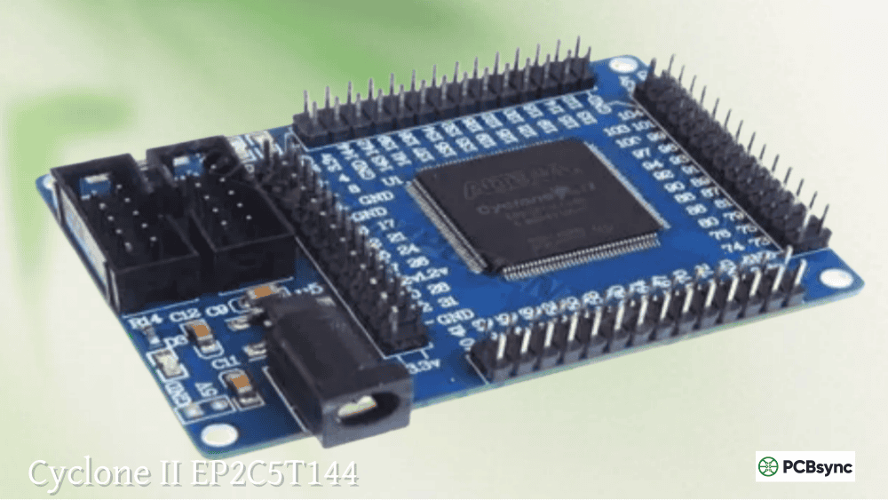
The EPCS1SI8N offers 1 Mbit (128 Kbytes) of storage in the smallest 8-pin SOIC package. This device supports Cyclone EP1C3 and EP1C4 devices comfortably, with the EP1C3 requiring approximately 630 Kbits uncompressed. With Cyclone’s built-in compression, even the EP1C6 can fit within the EPCS1 capacity.
The EPCS1 uses a simplified status register compared to larger family members. Block protection covers only four sectors, and the silicon ID operation returns 0x10 for device identification.
EPCS4SI8N Mid-Range Applications
Moving to 4 Mbit, the EPCS4SI8N handles Cyclone EP1C6, EP1C12, and most Cyclone II devices. The eight-sector architecture provides finer-grained protection options compared to EPCS1. This device remains popular for cost-sensitive industrial controllers where Cyclone II EP2C5 or EP2C8 devices provide sufficient logic resources.
EPCS16SI8N: The Industry Workhorse
The EPCS16SI8N earned its status as the default choice for mid-range FPGA designs through a combination of sufficient capacity, reasonable cost, and universal compatibility. At 16 Mbit, it accommodates:
All Cyclone devices (EP1C3 through EP1C20)
All Cyclone II devices (EP2C5 through EP2C70 with compression)
Most Cyclone III devices (EP3C5 through EP3C40)
Stratix II EP2S15 and EP2S30 (with compression)
The 32-sector organization enables flexible write protection schemes, useful when storing both FPGA configuration and user data in unused flash regions. Many designers use the Nios II processor to access spare EPCS capacity for parameter storage, boot logs, or field-updateable calibration data.
EPCS64SI16N for Larger FPGAs
When configuration files exceed 16 Mbit, the EPCS64SI16N steps in with 64 Mbit capacity in a 16-pin SOIC package. The larger package accommodates additional power and ground pins for improved signal integrity at 40 MHz operation.
The 128-sector memory organization provides extensive block protection options, documented in Table 3-12 of the configuration handbook.
EPCS128SI16N Maximum Capacity
For the largest legacy designs requiring more than 64 Mbit, the EPCS128SI16N provides 128 Mbit in the same 16-pin SOIC footprint. Note that this device uses a different identification scheme—it supports Read Device Identification (operation code 9Fh) rather than Read Silicon ID used by smaller devices.
Parallel Configuration Devices: EPC1PC8 and EPC16QC100N
Before serial configuration dominated, parallel devices like the EPC1PC8 and EPC16QC100N served older FPGA families. Understanding these remains relevant for legacy system maintenance.
EPC1PC8 Specifications
The EPC1PC8 provides 1 Mbit capacity in an 8-pin PDIP package operating at 5V. This device configures FLEX 6000, FLEX 10K, and ACEX 1K devices using passive serial (PS) or passive parallel (PP) schemes. Key characteristics:
Parameter
Specification
Capacity
1 Mbit
Package
8-pin PDIP
Supply Voltage
4.75V to 5.25V
Max Clock
16.7 MHz
Interface
Serial
Cascadable
Yes (with EPC2)
The EPC1PC8 can cascade with EPC2 devices for configurations exceeding 1 Mbit—a capability not available with EPCS serial devices.
EPC16QC100N Enhanced Configuration
The EPC16QC100N represents the enhanced configuration device family, offering 16 Mbit in a 100-pin PQFP package. This device supports both serial and fast parallel (FPP) configuration modes, achieving configuration times under 100ms for Stratix devices. The additional pins provide:
Successfully programming EPCS devices requires proper hardware setup, correct file generation, and understanding of the various programming modes.
Quartus Prime Software Configuration
Before programming, configure Quartus to target your specific EPCS device:
Open Assignments → Device → Device and Pin Options
Select the Configuration tab
Set Configuration device to match your hardware (EPCS16, EPCS64, etc.)
Set Configuration scheme to Active Serial
Recompile to generate the .pof file
The Quartus Programmer automatically generates Programmer Object Files (.pof) containing the configuration bitstream formatted for the selected device. For JTAG-based indirect programming, you’ll need a JTAG Indirect Configuration (.jic) file instead.
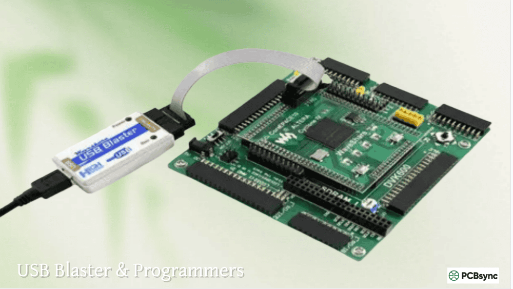
USB Blaster Programming Setup
The Intel FPGA Download Cable (USB Blaster) provides the primary in-system programming interface:
JTAG Mode (Direct FPGA Programming):
Mode: JTAG
File: .sof (SRAM Object File)
Result: Volatile—lost at power-down
Active Serial Mode (EPCS Programming):
Mode: Active Serial Programming
File: .pof (Programmer Object File)
Result: Non-volatile—survives power cycles
The critical distinction: JTAG mode programs the FPGA directly but doesn’t touch the EPCS device. Active Serial mode programs the EPCS through the FPGA’s AS interface pins.
Converting Files for Indirect Programming
When programming EPCS devices through the FPGA’s JTAG port (rather than direct AS connection), generate a .jic file:
Select File → Convert Programming Files
Set Programming file type to JTAG Indirect Configuration File (.jic)
Set Configuration device to your EPCS part number
Add your .sof file under SOF Data
Add your FPGA under Flash Loader
Generate the file
The .jic file bundles the FPGA bitstream with a temporary flash loader design. During programming, Quartus loads the flash loader into the FPGA, which then programs the EPCS device through the AS interface.
Command-Line Programming with quartus_pgm
For automated production programming, use the Quartus command-line programmer:
The -c parameter specifies the programming cable, -m sets the mode, and -o defines the operation (P=program, V=verify, E=erase).
PCB Design Guidelines for EPCS Devices
Proper PCB layout ensures reliable configuration across temperature, voltage, and manufacturing variations.
EPCS16SI8N Pinout and Connections
Pin
Name
Function
Connection
1
nCS
Chip Select (active low)
FPGA nCSO
2
DATA
Serial Data Output
FPGA DATA0
3
NC
No Connect
Leave floating
4
GND
Ground
Ground plane
5
ASDI
Serial Data Input
FPGA ASDO
6
NC
No Connect
Leave floating
7
DCLK
Serial Clock
FPGA DCLK
8
VCC
Power Supply
3.3V
EPCS64SI16N Pinout (16-Pin SOIC)
Pin
Name
Function
1
VCC
Power Supply (3.3V)
2
NC
No Connect
3
NC
No Connect
4
NC
No Connect
5
NC
No Connect
6
NC
No Connect
7
nCS
Chip Select
8
DATA
Serial Data Output
9
NC
No Connect
10
GND
Ground
11
NC
No Connect
12
NC
No Connect
13
NC
No Connect
14
NC
No Connect
15
ASDI
Serial Data Input
16
DCLK
Serial Clock
Power Supply Decoupling
Place a 100nF ceramic capacitor within 5mm of the VCC pin, connected directly to the ground plane via a short trace or via. For designs with long power distribution paths, add a 10µF tantalum or ceramic capacitor nearby.
The EPCS family operates from 2.7V to 3.6V, with 3.3V nominal. Current consumption during configuration reaches 15mA for 8-pin devices and 20mA for 16-pin variants.
Signal Integrity Considerations
Keep trace lengths under 6 inches for all signals. Match trace lengths between DATA, DCLK, ASDI, and nCS within 0.5 inches to prevent timing issues at higher clock frequencies.
For 40 MHz DCLK operation with EPCS16/64/128:
Maintain 50-ohm characteristic impedance on all signals
Avoid routing adjacent to high-speed digital or switching power signals
Use ground plane reference for all traces
Consider series termination resistors (22-33 ohms) at the FPGA output for long traces
Migrating Between EPCQL256 and EPCQL512 Quad-Serial Devices
Modern designs increasingly use EPCQ-L quad-serial devices for faster configuration. Understanding migration between EPCS and EPCQ families helps plan device upgrades.
EPCQL256 and EPCQL512 Key Features
Feature
EPCQL256
EPCQL512
Density
256 Mbit
512 Mbit
Package
FBGA-24
FBGA-24
Supply Voltage
1.8V
1.8V
AS x1 Mode
Yes
Yes
AS x4 Mode
Yes
Yes
Max DCLK (x1)
100 MHz
100 MHz
Max DCLK (x4)
100 MHz
100 MHz
The EPCQL256 and EPCQL512 operate at 1.8V—incompatible with older 3.3V EPCS devices. However, many Cyclone V and newer FPGAs support both voltage levels on configuration pins, allowing migration with appropriate level-shifting or bank voltage configuration.
Quad-serial mode (AS x4) increases effective bandwidth by 4x compared to EPCS, reducing configuration time for large devices. This requires four data pins (DATA[3:0]) instead of the single DATA0 used by EPCS devices.
Memory Organization and Sector Protection
Understanding the internal memory architecture helps when implementing field updates or storing user data alongside configuration bitstreams.
Sector-Based Architecture
EPCS devices organize memory into 64KB sectors, with the number of sectors scaling with device density:
Device
Total Sectors
Sector Size
Total Capacity
EPCS1SI8N
4
64 KB
256 KB (1 Mbit)
EPCS4SI8N
8
64 KB
512 KB (4 Mbit)
EPCS16SI8N
32
64 KB
2 MB (16 Mbit)
EPCS64SI16N
128
64 KB
8 MB (64 Mbit)
EPCS128SI16N
256
64 KB
16 MB (128 Mbit)
Each sector can be individually erased—a critical feature for field updates. However, you cannot erase individual bytes or pages; the entire 64KB sector must be erased before writing new data. This affects how you structure data storage when combining FPGA configuration with user parameters.
Block Protection Implementation
The status register contains block protection bits (BP0, BP1, BP2) that write-protect portions of the memory array. Protection starts from the top of memory and extends downward:
EPCS16SI8N Protection Levels:
BP2
BP1
BP0
Protected Sectors
Protected Range
0
0
0
None
No protection
0
0
1
Sector 31
Top 64KB
0
1
0
Sectors 30-31
Top 128KB
0
1
1
Sectors 28-31
Top 256KB
1
0
0
Sectors 24-31
Top 512KB
1
0
1
Sectors 16-31
Top 1MB
1
1
0
Sectors 0-31
All protected
1
1
1
Sectors 0-31
All protected
Protection prevents accidental erasure of critical data during field updates. A common strategy places the FPGA configuration in protected sectors and reserves unprotected sectors for user data that changes during operation.
Write and Erase Timing
Programming operations have specific timing requirements that affect production throughput:
Operation
EPCS1/4/16
EPCS64/128
Page Program (256 bytes)
5 ms max
5 ms max
Sector Erase (64 KB)
3 s max
3 s max
Bulk Erase
20 s max
250 s max
Write Status Register
15 ms max
15 ms max
Bulk erase on EPCS64SI16N and EPCS128SI16N takes significantly longer than smaller devices. For production programming, consider sector-by-sector erase with verification rather than bulk erase to reduce total programming time when only partial updates are needed.
Embedded Programming with SRunner
For systems requiring field updates without external programming equipment, Intel provides the SRunner software driver for embedded EPCS programming.
SRunner Architecture
SRunner implements the complete EPCS programming protocol in firmware, allowing a Nios II processor (or any microcontroller with SPI access) to reprogram the configuration device. The software reads Raw Programming Data (.rpd) files and handles:
Device identification and verification
Sector erase with progress tracking
Page programming with automatic address increment
Read-back verification
Status monitoring and error reporting
Implementation Requirements
To implement SRunner in your system:
Hardware Interface: Connect the EPCS to either dedicated FPGA pins or a general-purpose SPI controller
Memory for .rpd File: Provide sufficient storage for the new configuration (external flash, SD card, or network transfer)
Dual-Boot Capability: Implement a factory-safe boot image to recover from failed updates
Watchdog Protection: Use hardware watchdog to prevent bricked systems from incomplete updates
Typical Update Sequence
1. Receive new .rpd file via network/USB/serial
2. Validate file checksum
3. Disable interrupts and cache
4. Erase required sectors
5. Program new configuration data
6. Verify programmed data
7. Update configuration pointer (if using multi-boot)
8. Reset system to load new configuration
The entire process typically completes in 30-60 seconds for a 16 Mbit configuration, depending on interface speed and verification requirements.
Troubleshooting Common EPCS Programming Issues
Years of field experience reveal recurring problems with predictable solutions.
Silicon ID Recognition Failures
Symptom: “Can’t recognize silicon ID for device” error in Quartus Programmer
Causes and Solutions:
Wrong device selected – Verify the device in Quartus matches the actual EPCS part number on the board
MSEL configuration incorrect – Check MSEL pins match Active Serial mode for your FPGA family
Power supply issue – Measure VCC at the EPCS device during programming; must be 2.7V-3.6V
Signal integrity – Check for excessive noise on DCLK, ringing on control signals
Damaged device – EPCS flash has finite erase cycles (100,000+); replace if heavily used in development
Configuration Failure After Successful Programming
Symptom: Programming reports success, but FPGA doesn’t configure at power-up
Diagnostic Steps:
Verify CONF_DONE signal goes high after power-up (indicates successful configuration)
Check nSTATUS for error indication
Monitor DCLK during configuration—should show activity for expected duration
Verify all MSEL pins are correctly tied for AS mode
Check nCE (chip enable) is properly driven low
Intermittent Configuration Failures
Symptom: Configuration succeeds sometimes, fails other times
Common Causes:
Power supply sequencing issues—EPCS VCC must be stable before FPGA begins configuration
Temperature sensitivity—check operation across full temperature range
Signal integrity marginal at clock frequency—reduce DCLK if possible
High-volume manufacturing requires efficient programming strategies that balance throughput, reliability, and cost.
Gang Programming Options
For production volumes exceeding a few hundred units, gang programmers from BP Microsystems, System General, or Data I/O provide significant time savings. These systems program multiple devices simultaneously:
Programmer
Gang Sites
Supported Devices
Typical Throughput
BP-1610
16
EPCS1-128
400+ devices/hour
System General
8
EPCS1-128, EPCQ
200+ devices/hour
Data I/O
16+
All Intel config
500+ devices/hour
Pre-programming EPCS devices before board assembly eliminates in-circuit programming time and allows 100% device verification before placement.
In-Circuit Test Integration
When in-circuit programming is necessary, integrate programming into your ICT (In-Circuit Test) sequence:
Power-up board with controlled sequencing
Establish USB Blaster connection automatically
Program EPCS via Active Serial mode
Verify configuration using read-back comparison
Test FPGA functionality to confirm proper configuration
Log results with serial number tracking
Automated test equipment can execute the Quartus command-line programmer (quartus_pgm) as part of the test sequence, capturing pass/fail status and programming time metrics.
Environmental Screening
EPCS devices exhibit different programming characteristics across temperature. For high-reliability applications:
Program at room temperature (25°C) for consistent timing
Verify read-back at both temperature extremes
Allow additional margin on timing parameters for industrial temperature variants
Can I use an EPCQ device instead of EPCS for Cyclone IV?
Yes, EPCQ devices (including EPCQ16, EPCQ32, EPCQ64, EPCQ128, EPCQ256, and EPCQ512) can replace EPCS devices for Cyclone IV configuration. Both use the AS x1 protocol at the basic level. However, the pinout differs—EPCQ devices include additional pins for quad mode that must be properly terminated even when using single-bit mode. Refer to AN727 for detailed migration guidance.
Why won’t my EPCS device appear in the JTAG chain?
EPCS devices don’t have JTAG capability—they’re simple SPI flash memories without JTAG TAP controllers. You cannot directly see an EPCS in a JTAG scan. Instead, program EPCS devices either through Active Serial mode (direct connection to AS header) or JTAG indirect mode (programming through the FPGA using a .jic file). The FPGA’s flash loader IP temporarily loads into the FPGA and bridges JTAG commands to SPI operations.
What’s the difference between EPCS16SI8N and EPCS16SI16N?
Both are 16 Mbit EPCS devices. The EPCS16SI8N comes in an 8-pin SOIC package, while the EPCS16SI16N uses a 16-pin SOIC package. Functionally they’re identical—the 16-pin version simply has additional NC (no connect) pins and separate power/ground pins. The 8-pin version is more common and cost-effective for new designs. Choose the 16-pin version only if you need footprint compatibility with EPCS64 or EPCS128 for future density upgrades.
How do I access unused EPCS memory for data storage?
The Nios II processor ecosystem includes an EPCS controller IP that provides read/write access to EPCS flash through the Avalon memory-mapped interface. After configuration, the portion of EPCS memory not occupied by the bitstream remains available for user data. Typical applications include boot parameter storage, calibration data, and field-updateable lookup tables. Be careful with sector erase operations—erasing a sector containing configuration data will prevent FPGA boot.
Can EPCS devices be cascaded for larger configurations?
No, EPCS serial configuration devices cannot be cascaded. This is a fundamental limitation compared to older EPC parallel devices. If your configuration exceeds EPCS128 capacity (128 Mbit), consider EPCQ or EPCQ-L devices which offer up to 1 Gbit capacity, or enable bitstream compression in your FPGA (available for Stratix II and later, all Cyclone families). Compression typically achieves 40-60% size reduction, often allowing a smaller EPCS device than the uncompressed file size suggests.
Conclusion
The EPCS serial configuration family—from the compact EPCS1SI8N to the capacious EPCS128SI16N—provides reliable, cost-effective non-volatile storage for Intel FPGA bitstreams. While newer quad-serial devices like EPCQL256 and EPCQL512 offer faster configuration and higher density, EPCS devices remain the practical choice for Cyclone II, Cyclone III, and Cyclone IV designs where proven reliability and extensive documentation outweigh the benefits of newer technology.
Success with EPCS devices comes from understanding the AS protocol timing, following PCB layout guidelines, and maintaining proper power supply decoupling. When problems occur, systematic debugging using the MSEL configuration, signal integrity verification, and proper file generation usually identifies the root cause quickly.
For new designs targeting Cyclone V or later FPGAs, evaluate the EPCQ-L family for improved performance. For maintaining existing products or designing cost-sensitive systems with well-characterized Cyclone III/IV devices, the EPCS family remains an excellent choice backed by years of production history and comprehensive Intel support documentation.
Inquire: Call 0086-755-23203480, or reach out via the form below/your sales contact to discuss our design, manufacturing, and assembly capabilities.
Quote: Email your PCB files to Sales@pcbsync.com (Preferred for large files) or submit online. We will contact you promptly. Please ensure your email is correct.
Notes: For PCB fabrication, we require PCB design file in Gerber RS-274X format (most preferred), *.PCB/DDB (Protel, inform your program version) format or *.BRD (Eagle) format. For PCB assembly, we require PCB design file in above mentioned format, drilling file and BOM. Click to download BOM template To avoid file missing, please include all files into one folder and compress it into .zip or .rar format.


