Inquire: Call 0086-755-23203480, or reach out via the form below/your sales contact to discuss our design, manufacturing, and assembly capabilities.
Quote: Email your PCB files to Sales@pcbsync.com (Preferred for large files) or submit online. We will contact you promptly. Please ensure your email is correct.
Notes: For PCB fabrication, we require PCB design file in Gerber RS-274X format (most preferred), *.PCB/DDB (Protel, inform your program version) format or *.BRD (Eagle) format. For PCB assembly, we require PCB design file in above mentioned format, drilling file and BOM. Click to download BOM template To avoid file missing, please include all files into one folder and compress it into .zip or .rar format.
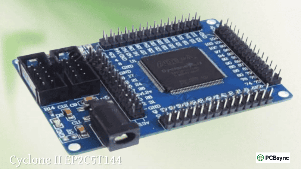
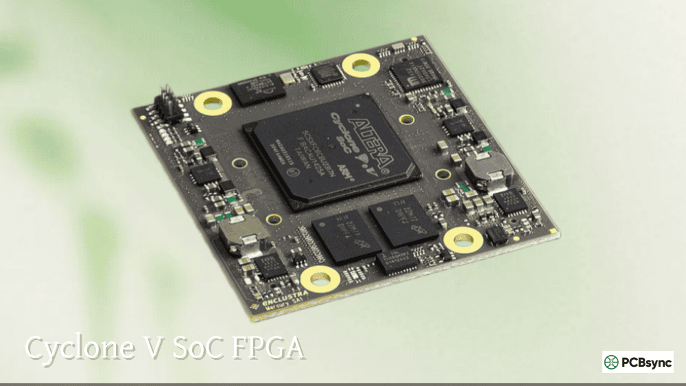
When I first encountered Altera ARM-based SoC FPGAs about six years ago, the learning curve felt vertical. Coming from pure FPGA development on Cyclone IV devices, suddenly dealing with U-Boot, device trees, and Linux kernel configurations alongside traditional RTL work was overwhelming. But once the pieces clicked together, the Cyclone V SoC became my go-to platform for complex embedded projects that needed both hard real-time control and sophisticated software processing.
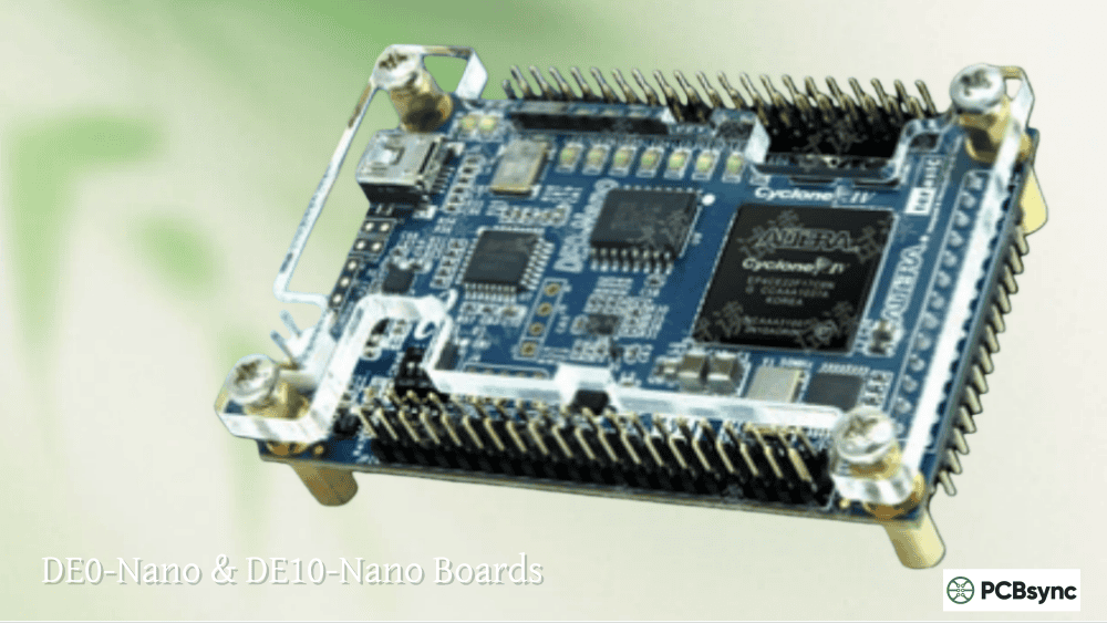
This guide consolidates practical knowledge from dozens of production designs—everything from industrial motor controllers to medical imaging systems—all built around devices like the 5CSEBA6U23I7NDK (DE10-Nano) and 5CSEMA4U23C6N (DE0-Nano-SoC). If you’re evaluating these parts for your next project or struggling to bridge the hardware-software divide, you’re in the right place.
Understanding the Intel Cyclone V SoC Architecture
The Cyclone V SoC family fundamentally differs from standard FPGAs by integrating a complete ARM Cortex-A9 MPCore processor system alongside traditional programmable logic. This isn’t a soft processor synthesized from logic cells—it’s hardened silicon running at up to 925 MHz, complete with its own DDR memory controller, cache hierarchy, and peripheral set.
Intel (formerly Altera) offers three SoC variants within the Cyclone V family:
Cyclone V SE SoC (5CSEA/5CSEBA Series)
The SE variants provide the ARM hard processor system (HPS) with general-purpose FPGA logic. Devices like the 5CEBA4F17C8N and 5CEBA4F17I7N fall into the non-SoC category (Cyclone V E), but the 5CSEBA5U23I7N and 5CSEBA6U23I7NDK integrate the full ARM subsystem. These are your workhorses for applications not requiring high-speed transceivers.
Cyclone V SX SoC (5CSXA/5CSXC Series)
The SX variants add 3.125 Gbps transceivers to the SE foundation. The 5CSXFC6D6F31C6N (found on the Cyclone V SX Development Kit) exemplifies this capability—useful when your design needs PCIe Gen2, SATA, or high-speed serial protocols alongside ARM processing.
Cyclone V ST SoC (5CSTFD Series)
At the top end, ST variants support 6.144 Gbps transceivers for applications demanding maximum serial bandwidth, such as CPRI fronthaul in telecommunications equipment.
Altera ARM Hard Processor System Deep Dive
The HPS within Cyclone V SoC devices represents a substantial embedded system independent of the FPGA fabric. Understanding its architecture is essential before attempting any development work.
Dual-Core ARM Cortex-A9 MPCore Processor
Each HPS contains either single or dual ARM Cortex-A9 cores operating at up to 925 MHz. The processor implements the ARMv7-A architecture with:
NEON SIMD engine for media processing
Single and double-precision floating-point unit
32KB L1 instruction cache and 32KB L1 data cache per core
Shared 512KB L2 cache with ECC support
Snoop Control Unit (SCU) managing cache coherency
Accelerator Coherency Port (ACP) allowing coherent FPGA fabric access
The 4,000+ DMIPS peak performance handles Linux distributions comfortably while leaving headroom for real-time tasks on the second core.
HPS Memory Subsystem
The hard memory controller supports DDR2, DDR3, and LPDDR2 SDRAM with data rates up to 400 MHz (800 Mbps). Key features include:
Feature
Specification
Interface Width
8, 16, 24, 32, or 40 bits
ECC Support
Optional with 8 or 16 additional bits
Max Addressable Memory
4 GB
Burst Length
4 or 8
ODT Support
Yes
The memory controller is shared between the ARM cores and FPGA fabric through a multiport front end (MPFE), enabling zero-copy data transfer between hardware accelerators and software.
Integrated Peripheral Controllers
The Altera ARM HPS includes an extensive peripheral set that eliminates external components from many designs:
Peripheral
Quantity
Key Features
Gigabit Ethernet (EMAC)
2
RGMII/SGMII, IEEE 1588 PTP support
USB 2.0 OTG
2
Host/Device/OTG modes
SD/SDIO/MMC
1
4-bit interface, boot capable
SPI Master
2
Quad SPI flash boot support
I2C
4
Standard and fast modes
UART
2
16550-compatible with FIFO
CAN
2
CAN 2.0B protocol
GPIO
Up to 67
Directly accessible or routed through FPGA
Watchdog Timer
2
System and processor watchdog
DMA Controller
8 channels
Peripheral and memory-to-memory
HPS-FPGA Communication Bridges
The real power of SoC FPGAs emerges from the high-bandwidth connections between the ARM processor and FPGA fabric. Three AXI bridges provide different access patterns:
HPS-to-FPGA Bridge (hps2fpga)
This 32, 64, or 128-bit wide AXI master interface allows the HPS to access memory-mapped peripherals implemented in FPGA logic. Running at up to 200 MHz in Cyclone V devices, peak bandwidth reaches 3.2 GB/s in 128-bit mode. Use this bridge for:
Control and status register access to custom IP
DMA transfers to FPGA-side buffers
Frame buffer access for display controllers
Lightweight HPS-to-FPGA Bridge (lwhps2fpga)
A 32-bit AXI master interface optimized for low-latency control register access. The reduced width simplifies FPGA interconnect at the cost of bandwidth—typically used for configuration registers rather than bulk data transfer.
FPGA-to-HPS Bridge (fpga2hps)
The reverse direction allows FPGA masters to access HPS memory and peripherals. This enables DMA engines in the FPGA fabric to directly write captured data into DDR memory accessible by Linux applications—critical for high-throughput data acquisition systems.
FPGA-to-HPS SDRAM Interface (fpga2sdram)
Direct FPGA access to the DDR memory controller bypasses the ARM caches entirely. Six ports with configurable width (16-256 bits) and independent command, read, and write channels provide massive bandwidth for video framebuffers or bulk data storage. Each port can achieve up to 6.4 GB/s throughput.
Cyclone V SoC Device Selection Guide
Choosing the correct device depends on your logic requirements, I/O count, and whether transceivers are needed. Here’s a practical comparison of common parts:
Cyclone V E (FPGA Only) Selection
Part Number
Logic Elements
M10K Blocks
User I/Os
Package
5CEBA4F17C8N
49,000
308
128
FBGA-256
5CEBA4F17I7N
49,000
308
128
FBGA-256 (Industrial)
5CEBA5F23C7N
77,000
397
224
FBGA-484
5CEBA9F31C8N
301,000
1,353
336
FBGA-896
Cyclone V SE SoC Selection
Part Number
Logic Elements
HPS Cores
User I/Os
Notes
5CSEMA4U23C6N
40,000
Dual-core
145
DE0-Nano-SoC
5CSEBA5U23I7N
85,000
Dual-core
145
Industrial temp
5CSEBA6U23I7NDK
110,000
Dual-core
145
DE10-Nano
5CSEA6U23I7
110,000
Dual-core
145
Production variant
The 5CSEBA6U23I7NDK and 5CSEMA4U23C6N are particularly popular because they appear on widely available development boards (DE10-Nano and DE0-Nano-SoC respectively), ensuring extensive community support and example projects.
Development Environment Setup
Successfully working with Cyclone V SoC requires both FPGA and embedded software toolchains. The learning curve is real, but proper setup makes it manageable.
Required Software Components
Intel Quartus Prime handles all FPGA-related tasks:
RTL synthesis and place-and-route
Platform Designer (Qsys) for system integration
SignalTap logic analyzer for FPGA debugging
Intel SoC EDS (Embedded Development Suite) provides ARM development tools:
ARM DS-5 (Development Studio) for debugging
GCC cross-compiler toolchain
BSP generator for bootloader creation
Hardware abstraction layer libraries
Linux Build Environment for creating the software stack:
Yocto Project / OpenEmbedded for custom distributions
Pre-built Linux images from RocketBoards.org
U-Boot bootloader sources
Installation Path
Install Quartus Prime (Lite edition works for Cyclone V SoC)
Ensure Cyclone V device support is included
Download and install SoC EDS matching your Quartus version
Set up a Linux VM or native installation for Yocto builds
The SoC EDS requires approximately 6-8 GB of disk space. Version 20.1 remains widely used, though newer releases continue to improve Agilex and Stratix 10 support.
Platform Designer System Architecture
Platform Designer (formerly Qsys) serves as the system integration environment where you connect the HPS to FPGA logic. A typical design follows this structure:
Essential Components
Every Cyclone V SoC design requires the Arria V/Cyclone V Hard Processor System component. This IP block configures:
HPS peripheral pinout (which signals route to dedicated pins vs. FPGA fabric)
Memory controller settings
Clock and reset configuration
Bridge enable/disable and width settings
Boot source selection
Connecting Custom IP
Custom FPGA peripherals typically connect through Avalon Memory-Mapped interfaces:
Create your custom IP with Avalon-MM slave interface
Add it to the Platform Designer system
Connect its clock and reset to appropriate sources
Connect its Avalon-MM slave to the hps_0.h2f_axi_master or hps_0.h2f_lw_axi_master
Assign a base address in the HPS address space
The Platform Designer automatically generates address maps and interconnect fabric. Export the system and synthesize to create the hardware design.
Boot Flow and Software Architecture
Understanding the Cyclone V SoC boot sequence clarifies many development challenges. The process involves multiple stages:
Stage 1: Boot ROM
On-chip ROM code executes immediately after reset. Based on BSEL pins (configured by board switches), it loads the next stage from:
QSPI flash
SD/MMC card
NAND flash
FPGA (via FPGA-to-HPS bridge)
Stage 2: Preloader/SPL
The Secondary Program Loader initializes DDR memory and loads U-Boot. For Cyclone V devices, the BSP Editor in SoC EDS generates this based on your Platform Designer handoff files. The preloader:
Configures PLL and clock settings
Initializes DDR memory controller
Optionally configures FPGA via FPGA Manager
Loads U-Boot into DDR and transfers control
Stage 3: U-Boot
Das U-Boot provides the boot environment, loading the Linux kernel and device tree from SD card or network. Configuration options include:
Kernel command line parameters
Boot device selection
FPGA configuration at boot time
Network boot (TFTP)
Stage 4: Linux Kernel
The kernel initializes all hardware using device tree descriptions, mounts the root filesystem, and starts userspace applications. For Cyclone V SoC, the linux-socfpga kernel fork includes drivers for:
FPGA Manager (dynamic reconfiguration)
HPS bridges (memory-mapped access from userspace)
All HPS peripherals
Practical Development Workflow
Here’s the workflow I’ve refined over numerous Altera ARM projects:
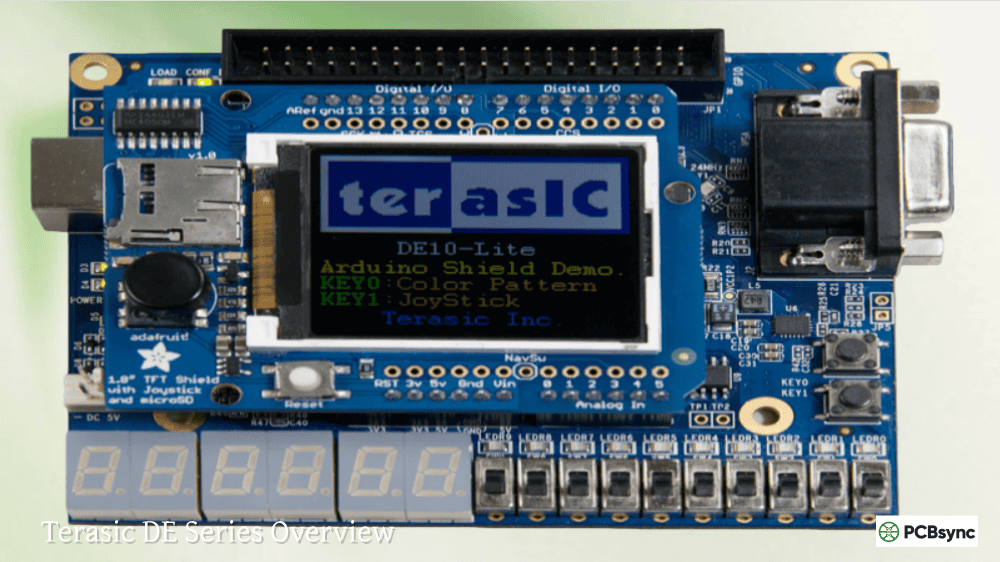
The DE10-Nano offers exceptional value for learning and prototyping. Its widespread adoption means abundant tutorials, example projects, and community support.
Cyclone V Device Datasheet: intel.com/programmable/technical-pdfs/683801.pdf
Cyclone V Hard Processor System Technical Reference Manual
Cyclone V Device Handbook Volume 1: Device Interfaces and Integration
AN 706: Mapping HPS IP Peripheral Signals to FPGA Interface
Advanced Development Topics
Dynamic Partial Reconfiguration
One compelling capability of the Cyclone V SoC platform involves runtime FPGA reconfiguration while the ARM processor continues executing. The FPGA Manager block enables partial reconfiguration scenarios where specific regions of the FPGA fabric can be updated without disturbing either the HPS or static FPGA logic.
Practical applications include:
Loading different hardware accelerators based on current processing needs
Field updates to custom IP without full system restart
A/B testing of logic implementations in production environments
Implementation requires careful design partitioning in Quartus Prime, defining static and reconfigurable regions. The linux-socfpga kernel provides the infrastructure through the FPGA Manager framework, allowing userspace applications to trigger reconfiguration.
Hardware-Software Co-Design Strategies
Successful Altera ARM SoC projects require thoughtful partitioning between HPS software and FPGA hardware. Consider these guidelines:
Move to FPGA when:
Real-time response under 10 microseconds is required
Parallel processing provides clear acceleration
Interface timing is critical (video, high-speed ADC)
Deterministic latency is mandatory
Keep in HPS software when:
Complex decision trees or state machines
Network protocol handling
Filesystem access
User interface implementation
Floating-point heavy algorithms (use NEON)
The AXI bridges provide sufficient bandwidth for most data movement, but minimize bridge crossings in latency-critical paths. Consider implementing complete processing pipelines entirely within FPGA fabric when timing permits.
Debugging Complex HPS-FPGA Systems
When hardware and software interact through multiple bridges and interrupt paths, debugging becomes challenging. A systematic approach helps:
SignalTap Integration
Intel’s embedded logic analyzer captures FPGA signals in real-time. For HPS-FPGA debugging:
Tap AXI bus signals at the bridge interface
Monitor custom IP control and status registers
Capture interrupt assertion and acknowledgment sequences
ARM DS-5 Software Debugging
The ARM Development Studio connects via JTAG to debug HPS software:
Set breakpoints in kernel drivers and userspace applications
Inspect memory-mapped FPGA registers
Profile execution timing
Cross-Trigger Interface (CTI)
The truly powerful debugging scenario connects SignalTap and DS-5 through CTI. An FPGA event (like a specific data pattern) can halt the ARM processor, or a software breakpoint can trigger SignalTap capture. This synchronized debugging is invaluable for race conditions and timing-sensitive bugs.
Performance Optimization Techniques
Maximizing throughput between HPS and FPGA requires understanding the interconnect architecture:
Bridge Selection Strategy
Scenario
Recommended Bridge
Reason
Bulk data transfer
fpga2sdram
Highest bandwidth, bypasses caches
Control registers
lwhps2fpga
Low latency, simple interconnect
Coherent DMA
ACP (via fpga2hps)
Cache coherency maintained
Frame buffers
fpga2sdram + hps2fpga
Write from FPGA, read from HPS
Burst Transactions
AXI burst transactions significantly improve throughput compared to single-beat transfers. When accessing sequential addresses, configure your FPGA IP to support burst lengths of 4, 8, or 16 beats. The M10K memory blocks naturally support burst access patterns.
Cache Considerations
For data shared between HPS and FPGA:
Use uncached mappings for control registers
Use cached mappings with explicit flush/invalidate for bulk data
Consider the ACP for cache-coherent FPGA access (adds latency but simplifies software)
Common Troubleshooting Scenarios
After supporting numerous Cyclone V SoC designs, certain problems appear repeatedly:
Boot Failure After Platform Designer Changes
Symptoms: Board doesn’t boot after modifying HPS configuration Solution: Regenerate the BSP after any Platform Designer change affecting HPS. The preloader uses handoff files that must match the actual FPGA configuration.
Bridge Timeout Errors
Symptoms: Linux reports AXI bus timeout, system hangs on FPGA access Causes:
FPGA not configured before HPS attempts bridge access
Clock domain crossing issues in custom IP
Address decoder misconfiguration
Solution: Ensure FPGA configuration completes before enabling bridges. Implement proper reset synchronization in custom IP.
Memory Access Violations
Symptoms: Segmentation fault or bus error accessing FPGA peripherals Causes:
Incorrect base address in software
mmap() size smaller than access range
Bridges not enabled in Platform Designer
Solution: Verify addresses match Platform Designer assignment. Check /sys/class/fpga_bridge/ status under Linux.
Interrupt Not Triggering
Symptoms: FPGA generates interrupt but HPS software never sees it Causes:
IRQ not connected in Platform Designer
Incorrect IRQ number in device tree
Interrupt controller configuration error
Solution: Trace interrupt path from FPGA IP through PIO/GIC to kernel. Verify device tree irq property matches Platform Designer assignment.
Frequently Asked Questions
What is the difference between 5CSEBA6U23I7N and 5CSEBA6U23I7NDK?
The ‘N’ suffix indicates RoHS-compliant lead-free packaging. The ‘DK’ suffix denotes an early development sample, sometimes called an engineering sample. In Quartus, you can target either 5CSEBA6U23I7N or 5CSEBA6U23I7—both will program identically to the 5CSEBA6U23I7NDK device. The parameters are identical; only the qualification status differs.
Can I use Quartus Prime Lite Edition for Cyclone V SoC development?
Yes, Quartus Prime Lite fully supports Cyclone V SoC devices including the 5CSEBA6U23I7NDK and 5CSEMA4U23C6N. The Lite edition lacks some advanced features like design partitioning and certain IP cores, but provides everything needed for most SoC development. However, SoC EDS requires separate installation regardless of which Quartus edition you use.
How do I configure the FPGA from the ARM processor at runtime?
The FPGA Manager subsystem allows the HPS to configure or reconfigure the FPGA fabric without external intervention. Under Linux, this is typically done through the /sys/class/fpga_manager interface or using the fpga_manager framework. The process involves: stopping any active HPS-FPGA communication, asserting FPGA reset, loading the .rbf file through the manager, and releasing reset. The rsYocto distribution simplifies this with command-line utilities.
What operating systems run on Cyclone V SoC devices?
The dual-core ARM Cortex-A9 supports:
Linux: Most common choice, with extensive support via linux-socfpga kernel
FreeRTOS: Real-time operating system for deterministic applications
Zephyr: Lightweight RTOS with growing Intel FPGA support
VxWorks: Commercial RTOS for safety-critical applications
Bare metal: Direct hardware access without OS overhead
Linux dominates for applications requiring networking, filesystems, and complex software stacks. FreeRTOS suits real-time control tasks where Linux’s non-deterministic scheduling is problematic.
Is the 5CEBA4F17C8N a SoC device with ARM processor?
No, the 5CEBA4F17C8N is a Cyclone V E (logic-only) FPGA without the ARM hard processor system. The part number structure differs: ‘5CEBA’ indicates Cyclone V E family, while ‘5CSEBA’ or ‘5CSEMA’ indicates Cyclone V SE SoC family. If you need the ARM Cortex-A9 processor, ensure your selected part number begins with ‘5CS’ (for SoC variants). The 5CEBA4F17I7N similarly lacks the HPS—it’s the industrial temperature variant of the same logic-only device.
Conclusion
The Intel Cyclone V SoC family represents a mature, well-documented platform for embedded designs requiring both programmable logic and general-purpose processing. Devices like the 5CSEBA6U23I7NDK and 5CSEMA4U23C6N deliver genuine heterogeneous computing—hardware acceleration where it matters most, with full Linux capability for complex software tasks.
The learning investment is substantial compared to pure FPGA development. You’ll need competence in RTL design, Platform Designer system integration, embedded Linux, and device driver development. But the payoff is significant: single-chip solutions replacing discrete processor and FPGA combinations, with bandwidth between domains that external interfaces simply cannot match.
Whether you’re building industrial automation controllers, software-defined radios, or edge computing platforms, the Altera ARM-based SoC provides the foundation. Start with a DE10-Nano or DE0-Nano-SoC board, work through the RocketBoards tutorials, and build your first HPS-FPGA bridge design. The complexity becomes manageable once you’ve completed that first successful boot.
Inquire: Call 0086-755-23203480, or reach out via the form below/your sales contact to discuss our design, manufacturing, and assembly capabilities.
Quote: Email your PCB files to Sales@pcbsync.com (Preferred for large files) or submit online. We will contact you promptly. Please ensure your email is correct.
Notes: For PCB fabrication, we require PCB design file in Gerber RS-274X format (most preferred), *.PCB/DDB (Protel, inform your program version) format or *.BRD (Eagle) format. For PCB assembly, we require PCB design file in above mentioned format, drilling file and BOM. Click to download BOM template To avoid file missing, please include all files into one folder and compress it into .zip or .rar format.


