Inquire: Call 0086-755-23203480, or reach out via the form below/your sales contact to discuss our design, manufacturing, and assembly capabilities.
Quote: Email your PCB files to Sales@pcbsync.com (Preferred for large files) or submit online. We will contact you promptly. Please ensure your email is correct.
Notes: For PCB fabrication, we require PCB design file in Gerber RS-274X format (most preferred), *.PCB/DDB (Protel, inform your program version) format or *.BRD (Eagle) format. For PCB assembly, we require PCB design file in above mentioned format, drilling file and BOM. Click to download BOM template To avoid file missing, please include all files into one folder and compress it into .zip or .rar format.
As a PCB engineer who’s spent countless hours debugging JTAG connections and wrestling with timing constraints, I can tell you that the Altera Cyclone IV FPGA family remains one of the most practical choices for getting into programmable logic development. Whether you’re picking up an EP4CE6E22C8N from AliExpress for under $40 or investing in a full-featured DE2-115 board with the EP4CE115F29C7, these devices offer an excellent balance of capability, cost, and community support.
This guide consolidates everything I’ve learned from real-world projects—from the initial Quartus setup headaches to finally achieving timing closure on a VGA controller. Let’s get into the specifics.
The Cyclone IV series from Intel (formerly Altera) represents the fourth generation of their cost-optimized FPGA line. Built on 60nm process technology, these devices target applications where power consumption and per-unit cost matter as much as raw performance. The family splits into two subfamilies: Cyclone IV E (general purpose) and Cyclone IV GX (with transceivers).
For most educational and prototyping work, the Cyclone IV E devices are what you’ll encounter. The EP4CE6 and EP4CE10 sit at the entry level, while the EP4CE115 represents the top end with over 114,000 logic elements.
What Makes Altera IV Cyclone Devices Popular
The Altera IV family hit a sweet spot that still resonates today. The EP4CE6E22C8N and EP4CE10E22C8N come in accessible TQFP-144 packages that even hobbyists can hand-solder in a pinch. More importantly, the Quartus Prime Lite edition supports these devices completely free of charge—no node-locked licenses, no feature restrictions that matter for learning.
I’ve worked with everything from Xilinx Spartan devices to Lattice iCE40 parts, and the Cyclone IV toolchain remains among the most beginner-friendly options available. The synthesis, place-and-route, and programming flow follows a logical progression that doesn’t require deep FPGA knowledge to get your first LED blinking.
EP4CE6 vs EP4CE10: Choosing Your Device
The question I get asked most often is whether to start with the EP4CE6 or upgrade to the EP4CE10. Here’s the practical breakdown based on actual project requirements:
Altera EP4CE6E22C8N Specifications
The EP4CE6 packs 6,272 logic elements into a compact package, which sounds limiting until you realize that’s enough for:
Multiple UART controllers
SPI and I2C masters
VGA display controllers (640×480)
Simple soft processors (not Nios II, but custom designs)
PWM generators for motor control
Basic DSP functions
The CoreEP4CE6 and similar low-cost boards based on the EP4CE6F17C8N (BGA package) or EP4CE6E22C8N (TQFP package) typically include 179 user I/Os, 270 Kbits of embedded memory, and 2 PLLs.
EP4CE10E22C8N: The Sweet Spot
The EP4CE10 bumps you up to 10,320 logic elements—roughly 65% more resources for typically less than $5 additional cost. This extra headroom becomes valuable when:
Your design approaches 70% utilization on the EP4CE6
You need more block RAM for frame buffers or FIFOs
Timing closure becomes difficult due to routing congestion
Both EP4CE6F17C8N and EP4CE10F17C8N share pin-to-pin compatibility in the BGA-256 package, allowing board designers to offer upgrade paths without PCB changes.
Cyclone IV E Device Comparison Table
Parameter
EP4CE6
EP4CE10
EP4CE15
EP4CE115
Logic Elements
6,272
10,320
15,408
114,480
Embedded Memory (Kbits)
270
414
504
3,888
M9K Memory Blocks
30
46
56
432
Embedded Multipliers (18×18)
15
23
56
266
PLLs
2
2
4
4
Max User I/Os
179
179
343
528
Global Clock Networks
10
10
20
20
Package Options
EQFP144, FBGA256
EQFP144, FBGA256, FBGA484
FBGA324, FBGA484
FBGA484, FBGA780
Development Board Options for Altera EP4CE6 and EP4CE10
The development board market for Cyclone IV devices ranges from $20 AliExpress specials to $600+ professional kits. Here’s what each tier actually delivers:
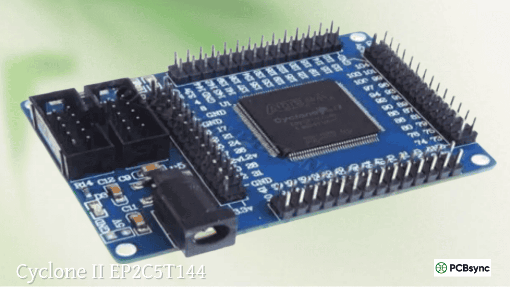
Budget Boards ($20-50): RZ-EasyFPGA and Clones
These boards built around the EP4CE6E22C8N or EP4CE10E22C8N typically include:
The documentation quality varies wildly. Some boards ship with Chinese-only manuals, while others have GitHub repositories with complete pinout files. Before purchasing, search for the specific board version plus “pinout” or “schematic” to verify community support exists.
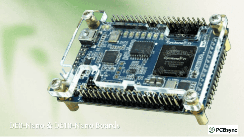
Mid-Range Boards ($80-200): Terasic DE0-Nano and Similar
The DE0-Nano uses an EP4CE22F17C6N, stepping up from the entry-level devices with more I/Os and a proper SDRAM chip. Key differences from budget boards:
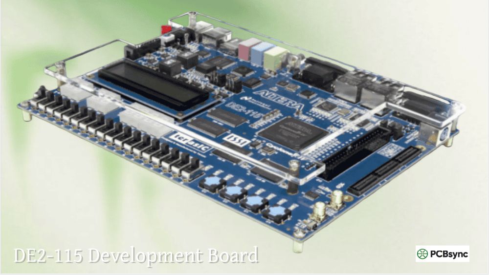
The DE2-115 represents the flagship Cyclone IV development platform. The EP4CE115F29C7 provides resources comparable to mid-range Virtex devices at a fraction of the cost. This board suits:
University courses requiring substantial project complexity
Power Supply Design Considerations for EP4CE FPGAs
The Cyclone IV power architecture requires careful attention. Getting this wrong causes mysterious programming failures or random behavior:
Voltage Rails Required
Rail
Voltage
Purpose
VCCINT
1.2V
Core logic
VCCIO
1.5V/1.8V/2.5V/3.3V
I/O banks (configurable)
VCCA
2.5V
PLL analog supply
VCCD_PLL
1.2V
PLL digital supply
The VCCA pins must be powered to 2.5V even if you’re not using PLLs. Leaving them floating causes configuration failures. Connect VCCD_PLL to VCCINT through a ferrite bead and decoupling capacitor.
Decoupling Strategy
Budget boards sometimes skimp on decoupling, leading to noise issues. For custom designs:
Place 100nF ceramic capacitors within 5mm of each power pin
Add 10µF bulk capacitors per voltage rail
Use 4.7µF ceramics near PLLs
Implement solid ground planes on all layers
FPGA Configuration Methods for EP4CE Devices
Cyclone IV devices support multiple configuration schemes. Understanding these prevents the “why won’t my design persist after power cycle” confusion:
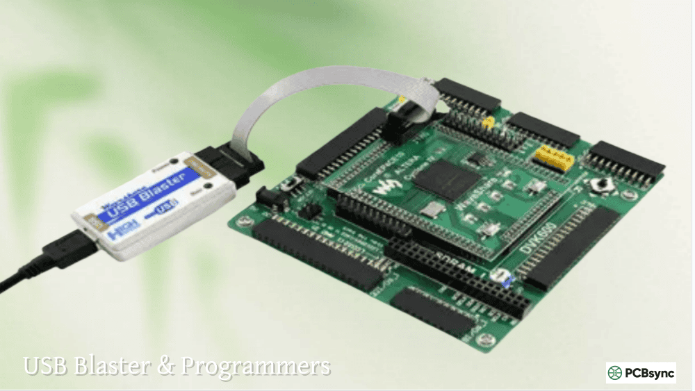
JTAG Programming (Volatile)
The fastest method during development. Downloads directly to SRAM configuration memory. Your design runs immediately but disappears when power is removed. Use this 99% of the time while developing.
Active Serial (AS) Programming
Programs the attached EPCS flash device. The FPGA loads this configuration automatically at power-up. Required for production or standalone operation. The EP4CE6 typically pairs with EPCS16 (16 Mbit) flash.
Passive Serial (PS) Configuration
An external microcontroller feeds configuration data to the FPGA. Used in systems where the MCU needs to control which configuration loads.
Creating JIC Files for Non-Volatile Storage
To generate a JTAG Indirect Configuration file:
File → Convert Programming Files
Select JTAG Indirect Configuration File (.jic)
Choose your configuration flash (EPCS16, EPCQ16, etc.)
Add the .sof file from your output directory
Generate and program via JTAG
This programs both the FPGA (temporarily) and the flash device through the JTAG chain.
Common Altera EP4CE Development Projects
The EP4CE6 and EP4CE10 handle a surprising range of applications. Here are proven project categories with resource estimates:
VGA Display Controller
A 640×480 VGA controller with a simple frame buffer typically consumes:
~500 logic elements for timing generation
~2,000 logic elements with text overlay
16-32 M9K blocks for frame buffer
The EP4CE6 handles this comfortably. Budget boards with resistor-DAC VGA output provide 3-bit-per-channel color (512 colors).
UART Communication Systems
A full-duplex UART with configurable baud rate uses approximately:
~200 logic elements per channel
1-2 M9K blocks for TX/RX FIFOs
You can implement 4+ UART channels in an EP4CE6 with room to spare.
I2C and SPI Controllers
Standard serial interfaces for sensor integration:
I2C master: ~150-300 logic elements
SPI master: ~100-200 logic elements
Multi-slave SPI: ~300-500 logic elements
Simple Soft Processors
While Nios II requires EP4CE22 minimum (practically), simpler 8-bit soft processors fit the EP4CE6:
MCPU (minimal CPU): ~400 logic elements
J1 Forth processor: ~600 logic elements
Custom state machines: varies widely
Troubleshooting Common EP4CE FPGA Issues
After debugging hundreds of student boards, these problems appear most frequently:
“Unable to scan device chain”
Check USB Blaster connection and drivers
Verify JTAG chain continuity (some boards have jumpers)
Ensure 3.3V is present on FPGA
Try reducing JTAG clock frequency in programmer settings
Configuration Fails or Doesn’t Persist
VCCA must be 2.5V (not optional)
Check EPCS flash is properly connected
Verify nCONFIG pull-up resistor present
Ensure MSEL pins match intended configuration scheme
Design Works in Simulation but Fails on Hardware
Add proper timing constraints (.sdc file)
Check for clock domain crossing issues
Verify I/O voltage standards match board hardware
Look for unregistered combinational paths
Timing Closure Failures
Reduce clock frequency to verify functionality
Add pipeline registers in critical paths
Use dedicated hardware multipliers instead of LUT-based
Consider spreading logic across more of the device
Step-by-Step Development Workflow for EP4CE FPGA Projects
Let me walk you through the actual workflow I use when starting a new Cyclone IV project. This process applies whether you’re using an EP4CE6E22C8N budget board or the EP4CE115F23C8N on a DE2-115.
Phase 1: Project Setup and Pin Planning
Before writing any HDL code, spend time understanding your target board’s pinout. This prevents the frustrating situation where your synthesized design won’t fit because you’ve assigned incompatible I/O standards to pins sharing the same VCCIO bank.
For budget EP4CE6 boards, I maintain a spreadsheet tracking:
Physical connector pin numbers
FPGA pin assignments
I/O bank membership
Maximum toggle rate for each pin
Special function availability (clock inputs, configuration pins)
The Altera EP4CE6 and EP4CE10 devices organize I/Os into 8 banks. Each bank shares a single VCCIO supply, meaning all pins in that bank must use compatible voltage standards. Mixing 3.3V LVTTL and 2.5V LVCMOS outputs in the same bank won’t work.
Phase 2: HDL Development and Simulation
Write your Verilog or VHDL with synthesis in mind from the start. Some constructs that simulate perfectly will consume excessive resources or fail timing when synthesized:
Avoid division operators (use shifts or DSP blocks for known divisors)
Initialize registers explicitly—don’t rely on default values
Use synchronous resets aligned to your clock domain
With a clean timing analysis report (no failing paths), program your device via JTAG and verify functionality. Use SignalTap II or external test equipment to observe internal signals. Common verification techniques:
LED indicators for state machine debugging
UART output for data logging
SignalTap capture of high-speed signals
Oscilloscope probing of I/O pins
Phase 5: Optimization and Iteration
Real designs rarely work perfectly on the first attempt. Iterative refinement addresses:
Timing violations through pipelining or logic restructuring
Resource constraints through sharing or algorithm optimization
Power consumption through clock gating or reduced switching activity
PCB Design Guidelines for Altera Cyclone IV FPGAs
When designing custom boards around the EP4CE6F17C8N or larger devices, follow these guidelines learned from production experience:
Layer Stackup Recommendations
Device Size
Minimum Layers
Recommended Stackup
EP4CE6
4
Signal-GND-Power-Signal
EP4CE10/EP4CE15
4-6
Signal-GND-Signal-Power-GND-Signal
EP4CE115
6-8
More complex with split power planes
Budget constraints sometimes force 4-layer designs for EP4CE6 boards. This works if you maintain solid ground planes and keep high-speed traces short.
Power Integrity Considerations
The EP4CE devices draw significant transient current during logic transitions. Inadequate power delivery causes:
Random configuration failures
Timing variations under load
Signal integrity degradation
Increased EMI emissions
Place bulk capacitors (47µF-100µF tantalum or polymer) near power entry points. Distribute ceramic capacitors (100nF) at each power pin. Add 10µF ceramics every 10mm along power rails for larger devices.
Signal Integrity for High-Speed Interfaces
When implementing high-speed interfaces like SDRAM or Ethernet on EP4CE designs:
Match trace lengths within 100 mils for parallel buses
Use series termination (22-33Ω) for heavily loaded outputs
Place clock signals on inner layers shielded by ground planes
Avoid routing signals over split planes
Configuration Circuit Design
The configuration interface connects your EPCS flash or USB Blaster to the FPGA. Critical considerations:
Keep DCLK trace short and well-referenced to ground
Add 10kΩ pull-up on nCONFIG
Provide 4.7kΩ pull-up on nSTATUS and CONF_DONE
Route data lines as matched-length differential pairs for high-speed AS modes
Advanced Development Topics for EP4CE Devices
Using Embedded Multipliers for DSP Applications
The Cyclone IV E family includes dedicated 18×18 multipliers that significantly outperform LUT-based implementations. The EP4CE6 provides 15 multipliers, while the EP4CE10 offers 23.
Instantiate multipliers directly for maximum control:
lpm_mult mult_inst (
.dataa(input_a),
.datab(input_b),
.result(product)
);
defparam mult_inst.lpm_widtha = 18;
defparam mult_inst.lpm_widthb = 18;
defparam mult_inst.lpm_widthp = 36;
defparam mult_inst.lpm_representation = “SIGNED”;
Each multiplier can run at 300+ MHz, enabling impressive DSP performance from these low-cost devices.
Memory Architecture and Usage
The M9K blocks (9,216 bits each) provide flexible on-chip memory. Configuration options include:
Single-port RAM
Simple dual-port RAM
True dual-port RAM
ROM (initialized during configuration)
Shift registers
FIFO buffers
The MegaWizard Plugin Manager generates optimized memory blocks with proper timing interfaces. For EP4CE6 designs needing larger buffers, external SDRAM or SRAM extends capacity significantly.
PLL Configuration for Clock Management
Both EP4CE6 and EP4CE10 include 2 PLLs capable of:
Frequency multiplication (up to 10×)
Frequency division
Phase shifting
Duty cycle adjustment
Spread-spectrum clock generation
A typical PLL configuration generates multiple clock domains from a single input:
altpll pll_inst (
.inclk0(clk_50),
.c0(clk_100), // 100 MHz for logic
.c1(clk_25), // 25 MHz for VGA
.c2(clk_12_5), // 12.5 MHz for UART
.locked(pll_locked)
);
Always wait for the locked signal before releasing system reset.
Migrating Between Altera IV EP4CE Devices
A well-designed project migrates smoothly between EP4CE family members. The pin-to-pin compatibility between EP4CE6F17C8N and EP4CE10F17C8N in the FBGA-256 package allows direct swap without PCB changes.
Migration Checklist
Verify package compatibility – Same package required for drop-in replacement
Check resource usage – Target device must exceed current utilization
Update Quartus project settings – Change device selection in assignment menu
Re-run synthesis and timing analysis – Different devices have different timing characteristics
Verify power requirements – Larger devices may draw more current
When to Consider Cyclone V Migration
If your EP4CE design pushes resource limits consistently, evaluate Cyclone V E devices:
2× logic density in similar packages
Improved timing performance
Enhanced DSP capabilities
Hard memory controllers
Better power efficiency
The Cyclone V toolflow in Quartus Prime closely resembles Cyclone IV, minimizing learning curve for the transition.
Comparing EP4CE6/EP4CE10 with Alternatives
How does the Cyclone IV stack up against modern alternatives?
Feature
Cyclone IV EP4CE10
Lattice iCE40UP5K
MAX10 10M08
Cyclone V E
Logic Elements
10,320
5,280
8,000
25,000+
Embedded Memory
414 Kb
1,024 Kb
378 Kb
1,760 Kb
Open-Source Tools
Limited
Yes (Yosys)
No
No
Cost (Dev Board)
$25-50
$30-50
$50-100
$100+
Learning Resources
Excellent
Good
Good
Good
Max Clock (typical)
300+ MHz
48 MHz
300+ MHz
450+ MHz
The Cyclone IV remains relevant despite its age primarily due to extensive documentation, low-cost boards, and mature tooling. For new designs requiring longevity, consider the MAX10 or Cyclone V families.
Essential Resources and Downloads
Official Documentation
Cyclone IV Device Handbook – Complete reference for device architecture, I/O standards, and configuration
Cyclone IV Device Datasheet – Electrical specifications, timing parameters, and package information
Quartus Prime Handbook – Comprehensive IDE and toolflow documentation
GitHub repositories – Search “Cyclone IV” for example projects
OpenCores – Free IP cores compatible with Cyclone IV
FPGA subreddit – Active community discussion
Frequently Asked Questions
What is the difference between EP4CE6E22C8N and EP4CE6F17C8N?
The package type differs: E22 indicates EQFP-144 (easy to solder), while F17 indicates FBGA-256 (more I/Os but requires reflow soldering). Both contain identical FPGA dies with 6,272 logic elements. The ‘C8’ suffix indicates commercial temperature grade (0°C to 85°C) and -8 speed grade. The ‘N’ suffix denotes lead-free (RoHS compliant) packaging.
Can I run Nios II soft processor on the EP4CE6?
Technically possible but extremely constrained. The EP4CE6 provides insufficient resources for practical Nios II deployment—you’ll hit memory and logic limits immediately. Use EP4CE22 minimum, preferably EP4CE55 or larger. For soft processor work on a budget, consider the DE0-Nano or similar EP4CE22-based boards.
Which Quartus version supports Cyclone IV?
Quartus Prime Lite and Standard editions continue to support Cyclone IV through version 23.1 and beyond. Intel has placed these tools in “maintenance mode,” meaning no new features but continued bug fixes. Cyclone IV isn’t going away—these devices remain in active production.
Is the Altera Cyclone IV still relevant for new designs?
For educational purposes, prototyping, and low-volume production, absolutely. The combination of free tools, extensive documentation, and affordable development boards makes Cyclone IV ideal for learning. For new commercial products requiring 5+ year availability, evaluate MAX10 or Cyclone 10 LP as migration targets with similar architecture.
How do EP4CGX devices differ from EP4CE?
The EP4CGX series (Cyclone IV GX) adds high-speed transceivers for protocols like PCIe and Gigabit Ethernet. The EP4CE series lacks these transceivers but costs less. For designs not requiring dedicated high-speed serial interfaces, the EP4CE family provides better value.
Conclusion
The Cyclone IV FPGA family, particularly the EP4CE6E22C8N and EP4CE10E22C8N, continues to offer an unmatched entry point into FPGA development. The devices themselves are mature and well-understood, the tools are free and capable, and the community has produced extensive learning materials.
Whether you’re a student working through digital design coursework, a hobbyist building custom peripherals, or an engineer prototyping a new product concept, these Altera IV devices deliver the right balance of capability and accessibility. Start with the EP4CE6 to learn the toolflow and fundamental concepts, upgrade to EP4CE10 when you need breathing room, and graduate to EP4CE115 or Cyclone V when your projects demand serious resources.
The path from blinking LEDs to complex embedded systems runs directly through these devices. Get a cheap development board, install Quartus, and start experimenting—that’s still the best way to learn FPGA development.
Inquire: Call 0086-755-23203480, or reach out via the form below/your sales contact to discuss our design, manufacturing, and assembly capabilities.
Quote: Email your PCB files to Sales@pcbsync.com (Preferred for large files) or submit online. We will contact you promptly. Please ensure your email is correct.
Notes: For PCB fabrication, we require PCB design file in Gerber RS-274X format (most preferred), *.PCB/DDB (Protel, inform your program version) format or *.BRD (Eagle) format. For PCB assembly, we require PCB design file in above mentioned format, drilling file and BOM. Click to download BOM template To avoid file missing, please include all files into one folder and compress it into .zip or .rar format.


