Inquire: Call 0086-755-23203480, or reach out via the form below/your sales contact to discuss our design, manufacturing, and assembly capabilities.
Quote: Email your PCB files to Sales@pcbsync.com (Preferred for large files) or submit online. We will contact you promptly. Please ensure your email is correct.
Notes: For PCB fabrication, we require PCB design file in Gerber RS-274X format (most preferred), *.PCB/DDB (Protel, inform your program version) format or *.BRD (Eagle) format. For PCB assembly, we require PCB design file in above mentioned format, drilling file and BOM. Click to download BOM template To avoid file missing, please include all files into one folder and compress it into .zip or .rar format.
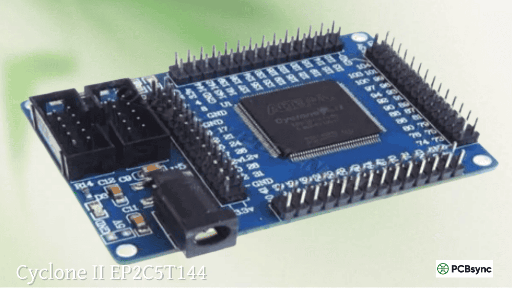
If you’re looking to break into FPGA development without spending hundreds of dollars on evaluation kits, the Altera EP2C5T144 development board is likely the most cost-effective entry point you’ll find. As someone who has introduced dozens of engineers and students to programmable logic, I’ve watched this little CycloneII EP2C5T144 board become the de facto starting point for FPGA education worldwide.
For under $20, you get a genuine Altera FPGA CycloneII EP2C5T144 with enough resources to learn digital design fundamentals, build practical projects, and even prototype commercial applications. This guide covers everything you need to know to get started—from understanding the hardware specifications to programming your first LED blink project.
The EP2C5T144 is an FPGA chip from Intel (formerly Altera) belonging to the Cyclone II family. Unlike microcontrollers that execute software instructions sequentially, FPGAs allow you to create actual digital hardware circuits through configuration. This fundamental difference opens up possibilities for parallel processing, custom peripheral implementations, and timing-critical applications that software simply cannot match.
The EP2C5 designation indicates the smallest member of the Cyclone II family, with the “T144” suffix referring to the 144-pin TQFP (Thin Quad Flat Package). Despite being the entry-level device, it packs serious capability into a compact package.
Cyclone II Family Overview
The CycloneII EP2C5T144 sits at the beginning of a scalable family. Understanding where it fits helps you plan upgrade paths as your projects grow:
Device
Logic Elements
M4K RAM Blocks
Total RAM Bits
Multipliers
PLLs
Max I/O
EP2C5
4,608
26
119,808
13
2
89
EP2C8
8,256
36
165,888
18
2
85-138
EP2C15
14,448
52
239,616
26
2
142-315
EP2C20
18,752
52
239,616
26
4
142-315
EP2C35
33,216
105
483,840
35
4
322-475
EP2C50
50,528
129
594,432
86
4
294-450
EP2C70
68,416
250
1,152,000
150
4
422-622
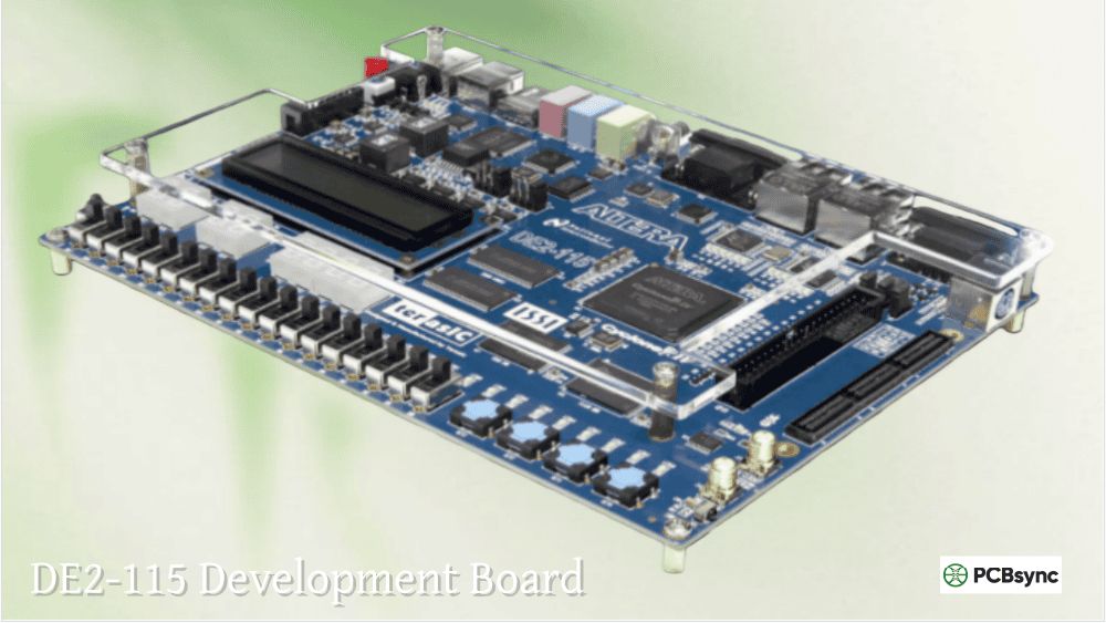
The EP2C8 offers nearly double the logic capacity if you outgrow the EP2C5, while the EP2C20F484C6N is popular on larger development boards like the DE1 and DE2 when you need substantial resources for complex designs.
EP2C5T144 Development Board Specifications
Most Altera EP2C5T144 development boards available from various vendors share a similar design. Here’s what you typically get:
Core FPGA Specifications
Parameter
Value
Device
EP2C5T144C8N
Logic Elements (LEs)
4,608
LE per LAB
16
Total LABs
288
M4K RAM Blocks
26
Total RAM Bits
119,808
Embedded Multipliers
13 (18×18) or 26 (9×9)
PLLs
2
Maximum User I/O
89
Core Voltage
1.2V
I/O Voltage
3.3V LVTTL
Package
144-pin TQFP
Speed Grade
-8 (commercial)
Development Board Features
The typical CycloneIIEP2C5T144 minimum system board includes:
To effectively use any FPGA, you need to understand its internal architecture. The Cyclone II EP2C5T144 uses Intel’s proven low-cost FPGA architecture optimized for cost-sensitive applications.
Logic Array Blocks (LABs)
The fundamental building block is the Logic Array Block (LAB), containing 16 Logic Elements (LEs). Each LE includes:
4-Input Look-Up Table (LUT): Can implement any 4-input Boolean function. This is where your combinational logic lives.
Programmable Register: Each LE contains a flip-flop that can be configured as D, T, JK, or SR type. The register features:
Data, clock, clock enable, and clear inputs
Synchronous load capability
Register bypass for purely combinational outputs
Carry Chain: Dedicated carry logic enables efficient implementation of arithmetic functions like adders and counters.
Register Chain: Allows registers to cascade within a LAB, useful for shift registers.
Embedded Memory
The 26 M4K blocks provide 119,808 bits of on-chip RAM. Each M4K block supports:
For a beginner, this embedded memory is useful for:
Video frame buffers (limited)
FIFOs for data rate matching
Look-up tables for math functions
Register files for soft processors
Embedded Multipliers
The 13 embedded multipliers can each perform 18×18-bit multiplication in a single clock cycle, or be split into two 9×9-bit multipliers. This makes the EP2C5T144 capable of basic DSP functions without consuming precious logic elements.
Phase-Locked Loops (PLLs)
Two PLLs enable clock management:
Clock multiplication and division
Phase shift adjustment
Spread-spectrum clocking
Up to 5 output clocks per PLL
Input frequency range: 16MHz to 500MHz
The 50MHz on-board oscillator can be multiplied up or divided down as needed for your design.
Getting Started: Required Equipment
Before diving into your first project, gather these essentials:
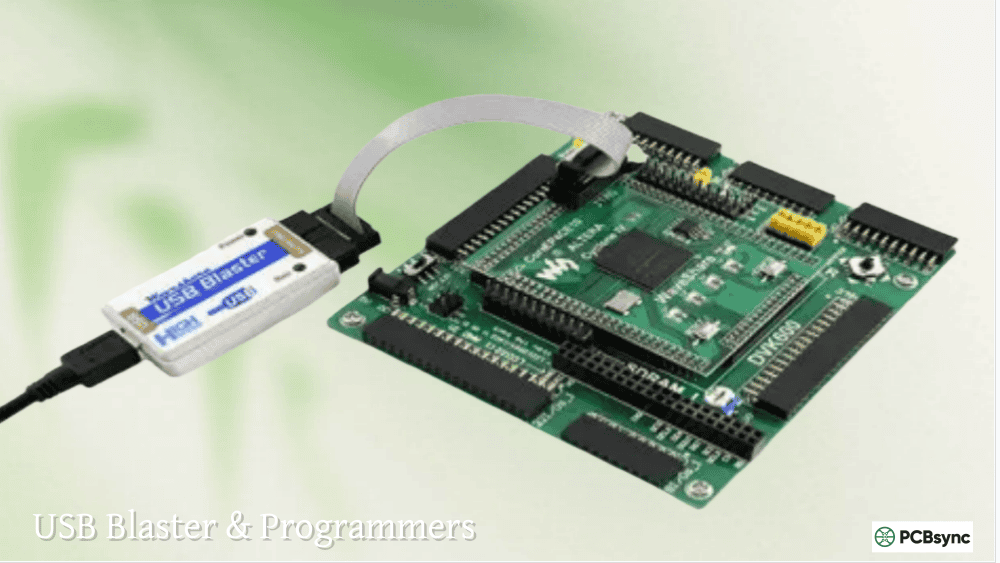
Note on USB Blasters: Both genuine Intel USB Blasters and clone versions work with the Altera EP2C5T144. The clones typically cost under $10 and function identically for programming purposes.
Software Requirements
The CycloneIIEP2C5T144 requires legacy Quartus II software since Intel discontinued support for Cyclone II in newer Quartus Prime versions.
Software
Version
Notes
Quartus II Web Edition
13.0sp1
Last version supporting Cyclone II
Cyclone II Device Support
13.0sp1
Download separately
ModelSim-Altera Starter
10.1d
Optional: for simulation
Download Links:
Quartus II 13.0sp1: http://fpgasoftware.intel.com/13.0sp1/
Device Support: Available from the same page
Pin Assignments for EP2C5T144 Development Board
Understanding the board’s pin mapping is crucial for successful projects. Here are the key assignments for the standard CycloneII EP2C5T144 minimum system board:
Fixed Pin Assignments
Function
Pin Number
Notes
50MHz Clock
PIN_17
On-board oscillator output
Reset Button
PIN_144
Active-low, directly usable
LED0
PIN_3
Active-high, directly usable
LED1
PIN_7
Active-high, directly usable
LED2
PIN_9
Active-high, directly usable
JTAG Interface Pins
Signal
Pin Number
TDI
PIN_14
TDO
PIN_79
TMS
PIN_15
TCK
PIN_16
Configuration Pins
Signal
Pin Number
Notes
nCONFIG
PIN_144
Directly usable
CONF_DONE
Dedicated
nSTATUS
Dedicated
DATA0
PIN_2
Directly usable
DCLK
PIN_1
Directly usable
nCSO
PIN_4
Directly usable
ASDO
PIN_5
Directly usable
I/O Banks and Available Pins
The EP2C5T144 organizes I/O into banks. All user I/O operates at 3.3V LVTTL levels on this development board:
Bank
Available Pins
Notes
Bank 1
Multiple
General I/O
Bank 2
Multiple
General I/O
Bank 3
Multiple
JTAG shared
Bank 4
Multiple
Configuration shared
Your First Project: LED Blink
Let’s walk through creating the classic “Hello World” of FPGA development—blinking an LED. This project verifies your entire toolchain works correctly.
Step 1: Create New Project in Quartus II
Launch Quartus II 13.0sp1
Select File → New Project Wizard
Set working directory (e.g., C:\FPGA\led_blink)
Project name: led_blink
Top-level entity: led_blink
Click Next
Step 2: Select the Device
Family: Cyclone II
Available devices: EP2C5T144C8
Click Next through remaining screens
Click Finish
Step 3: Create Verilog Source File
Select File → New → Verilog HDL File and enter this code:
module led_blink(
input wire clk, // 50MHz clock (PIN_17)
output reg [2:0] led // LEDs (PIN_3, PIN_7, PIN_9)
);
// 26-bit counter for timing
reg [25:0] counter;
always @(posedge clk) begin
counter <= counter + 1’b1;
// Toggle LEDs at different rates
led[0] <= counter[25]; // ~0.75 Hz
led[1] <= counter[24]; // ~1.5 Hz
led[2] <= counter[23]; // ~3 Hz
end
endmodule
Save as led_blink.v
Step 4: Assign Pins
Select Assignments → Pin Planner
Find your signals in the Node Name column
Assign locations:
Node Name
Location
clk
PIN_17
led[0]
PIN_3
led[1]
PIN_7
led[2]
PIN_9
Close Pin Planner
Step 5: Compile the Design
Select Processing → Start Compilation
Wait for compilation to complete (check for 0 errors)
Review the Compilation Report
Step 6: Program the FPGA
Connect USB Blaster to the JTAG header
Connect 5V power to the board
Select Tools → Programmer
Click Hardware Setup and select USB-Blaster
Click Auto Detect to find the EP2C5
Select your .sof file
Check Program/Configure
Click Start
If everything works, you’ll see the three LEDs blinking at different rates!
Step 7: Save to On-Board Flash (Permanent Programming)
The SRAM-based EP2C5T144 loses its configuration when power is removed. To make your design permanent:
Cyclone II Support Resources: https://www.intel.com/content/www/us/en/support/programmable/support-resources/devices/cyclone-ii-support.html
Datasheet Archive: https://www.alldatasheet.com – Search for EP2C5T144C8N
Community Resources
Resource
URL
Content
Intel FPGA Forums
community.intel.com
Official support
GitHub
Search “EP2C5T144”
Example projects
Hackaday
hackaday.io
Project inspiration
Land-Boards Wiki
land-boards.com
Pin assignments, examples
Frequently Asked Questions
What software version do I need for the EP2C5T144?
The EP2C5T144 and entire Cyclone II family require Quartus II 13.0sp1 or earlier. Intel discontinued Cyclone II support in Quartus Prime. Download the Web Edition (free) along with the Cyclone II device support package from Intel’s legacy software archive. Note that Quartus II 13.0sp1 runs on Windows 7/8/10 but may have compatibility issues with Windows 11—using compatibility mode usually resolves this.
Can the EP2C5T144 run a soft processor like NIOS II?
Yes, the Altera EP2C5T144 can run NIOS II/e (economy version). The /e core requires approximately 600-800 LEs, leaving room for peripherals and custom logic. However, with only 119Kb of on-chip RAM, you’ll need external memory for any substantial software. For serious embedded development, consider upgrading to an EP2C20F484C6N board which offers more resources.
Why does my design disappear when I power off the board?
Cyclone II FPGAs, including the CycloneII EP2C5T144, use SRAM-based configuration that requires reprogramming after power loss. To make your design permanent, program the on-board EPCS4 flash memory using Active Serial programming mode. Convert your .sof file to .jic format using the Convert Programming Files tool, then program via the AS header instead of JTAG.
What’s the difference between EP2C5T144C8 and EP2C5T144C8N?
The “N” suffix indicates RoHS compliance (lead-free). The EP2C5T144C8N is the lead-free version while EP2C5T144C8 uses traditional tin-lead solder. Functionally, they are identical—same logic capacity, same speed grade, same pinout. Modern boards use the N version exclusively for environmental compliance.
Can I use the EP2C5T144 for commercial products?
While the Altera FPGA CycloneII EP2C5T144 is technically capable of commercial deployment, Cyclone II is a legacy product family with limited long-term availability. Intel recommends MAX 10 or Cyclone 10 LP for new commercial designs. For learning, prototyping, and hobby projects, the EP2C5T144 remains excellent. For products requiring 5+ year availability, plan migration to current-generation devices.
Design Tips and Best Practices
After working with the EP2C5T144 on numerous projects, I’ve compiled practical advice that will save you time and frustration.
Clock Domain Management
The 50MHz on-board oscillator feeds PIN_17, but most designs need multiple clock frequencies. Use the PLLs rather than clock dividers:
Good Practice:
Use MegaWizard to instantiate ALTPLL
Generate required frequencies from 50MHz input
Let the PLL handle phase relationships
Avoid:
Dividing clocks with counters (creates clock domain crossing issues)
Using gated clocks (synthesis tools struggle with these)
Ignoring clock skew in timing analysis
Resource Optimization
With only 4,608 LEs, efficiency matters on the CycloneII EP2C5T144:
Logic Element Conservation:
Use embedded multipliers for any multiplication—they’re free
Store constants in M4K blocks rather than LUT-based ROM
Share arithmetic units with multiplexing when possible
Use the register chains for shift registers
Memory Usage:
Plan M4K allocation carefully—you only have 26 blocks
Use appropriate aspect ratios to minimize waste
Consider implementing small memories in distributed logic if M4K is constrained
Timing Closure
Even on this “slow” FPGA, timing closure matters:
Strategies:
Always run TimeQuest Timing Analyzer
Pipeline long combinational paths
Register all I/O (use IOE registers)
Constrain your clocks properly in SDC files
Power Considerations
The on-board regulators on typical Altera EP2C5T144 boards have limited current capacity:
Regulator
Typical Rating
Notes
3.3V
~500mA
Powers I/O banks
1.2V
~300mA
Powers core logic and PLLs
Complex designs with high switching activity may exceed these limits. Watch for:
Unexpected board heating
Unstable operation under load
Voltage drooping under heavy I/O activity
If you encounter power issues, consider external power through the header pins rather than the barrel jack.
Expanding Your EP2C5T144 System
The beauty of the Altera FPGA CycloneII EP2C5T144 board lies in its expansion capability. With 89 I/O pins broken out to standard headers, you can interface with virtually any external hardware.
Common Expansion Modules
Module Type
Interface
Pins Required
Notes
7-Segment Display (4-digit)
Parallel
8-12
Multiplexed driving
LCD Character Display
4-bit parallel
6-7
HD44780 compatible
VGA Output
RGB + Sync
5-15
Depends on color depth
PS/2 Keyboard/Mouse
Serial
2
Clock + Data
SPI Flash (extra)
SPI
4
For larger storage
I2C Devices
I2C
2
Many sensors available
SDRAM
Parallel
30+
Challenging but doable
Audio PWM
Single wire
1
Plus filter components
Building a Test Bench
For serious development, construct a permanent test setup:
Base Board: Solder the EP2C5T144 board to a prototyping PCB
Power Distribution: Add proper decoupling and bulk capacitors
I/O Headers: Bring signals to convenient test points
LED Array: Add 8 LEDs for debugging (active-low recommended)
DIP Switches: 8 switches for configuration inputs
Push Buttons: 4 debounced buttons for control
7-Segment Display: 4-digit multiplexed display
Serial Port: RS-232 level shifter for UART debugging
This test bench setup lets you quickly verify new designs without breadboard wiring for every project.
Interfacing with Modern Platforms
The CycloneIIEP2C5T144 connects well with modern development platforms:
When your projects outgrow the EP2C5, you have clear upgrade paths:
Staying with Cyclone II
The EP2C8 provides nearly double the logic elements while maintaining similar pricing and board availability. Pin compatibility within the same package family means your code ports easily.
The Altera Cyclone II EP2C5T144 development board represents perhaps the most accessible entry point into FPGA development. For roughly the price of a nice lunch, you get genuine Intel FPGA silicon with enough resources to learn digital design principles, implement real-world interfaces, and even prototype commercial applications.
While the Cyclone II family is now legacy hardware, the skills you develop—HDL coding, timing analysis, resource optimization, and hardware debugging—transfer directly to current-generation devices. The EP2C5T144 teaches you to work within constraints, a valuable skill when you eventually move to larger FPGAs where the temptation to waste resources grows.
Whether you’re a student learning digital design, a software engineer curious about hardware, or a hobbyist building custom electronics, the CycloneIIEP2C5T144 provides a solid foundation. Start with LED blinking, progress through increasingly complex projects, and before long you’ll understand why FPGA engineers get excited about programmable logic.
The best time to start learning FPGAs was yesterday. The second best time is right now—with an Altera EP2C5T144 board on your bench.
Inquire: Call 0086-755-23203480, or reach out via the form below/your sales contact to discuss our design, manufacturing, and assembly capabilities.
Quote: Email your PCB files to Sales@pcbsync.com (Preferred for large files) or submit online. We will contact you promptly. Please ensure your email is correct.
Notes: For PCB fabrication, we require PCB design file in Gerber RS-274X format (most preferred), *.PCB/DDB (Protel, inform your program version) format or *.BRD (Eagle) format. For PCB assembly, we require PCB design file in above mentioned format, drilling file and BOM. Click to download BOM template To avoid file missing, please include all files into one folder and compress it into .zip or .rar format.


