Inquire: Call 0086-755-23203480, or reach out via the form below/your sales contact to discuss our design, manufacturing, and assembly capabilities.
Quote: Email your PCB files to Sales@pcbsync.com (Preferred for large files) or submit online. We will contact you promptly. Please ensure your email is correct.
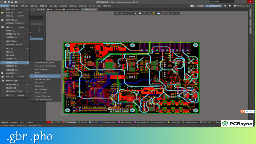
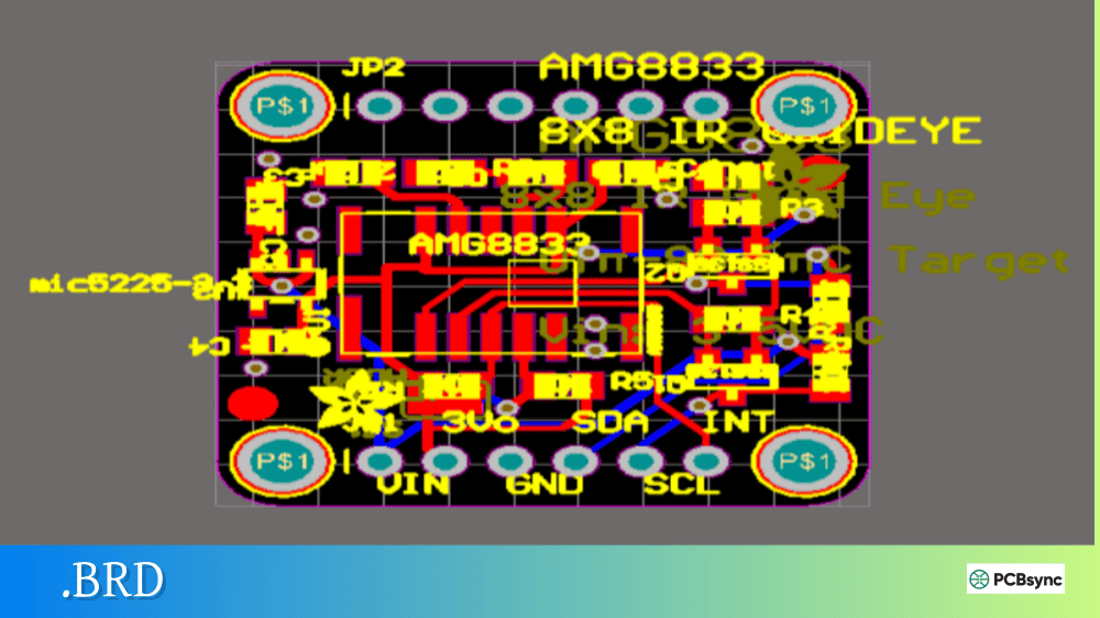
Notes: For PCB fabrication, we require PCB design file in Gerber RS-274X format (most preferred), *.PCB/DDB (Protel, inform your program version) format or *.BRD (Eagle) format. For PCB assembly, we require PCB design file in above mentioned format, drilling file and BOM. Click to download BOM template To avoid file missing, please include all files into one folder and compress it into .zip or .rar format.
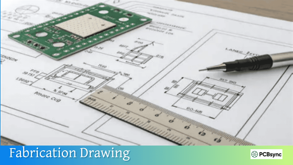
I learned early in my career that Gerber files alone don’t tell the whole story. After a manufacturer built my first multilayer board with the wrong stackup—because I assumed they’d figure it out from the layer count—I never made that mistake again. The fabrication drawing is where you communicate everything the Gerbers can’t convey, and getting it right saves weeks of back-and-forth engineering questions.
This guide covers everything you need to know about fabrication drawings, from the essential elements every fab drawing requires to the specific notes that prevent manufacturing errors.
A fabrication drawing is a detailed engineering document that provides all the manufacturing specifications needed to build a bare printed circuit board. While Gerber files define the copper patterns, solder mask, and silkscreen artwork, the fabrication drawing specifies the physical construction parameters: board thickness, layer stackup, drill sizes, material requirements, surface finish, and quality standards.
Think of it as the blueprint that accompanies your circuit artwork. The Gerbers show what the board looks like; the fabrication drawing tells the manufacturer how to build it. Without a complete fab drawing, manufacturers must make assumptions about your design intent—and those assumptions often lead to boards that don’t meet your requirements.
A fabrication drawing typically includes several components: the board outline with dimensions, a drill chart showing all hole sizes, a layer stackup diagram, and a comprehensive set of fabrication notes. Together, these elements give the PCB fabricator everything needed to quote, plan, and manufacture your board correctly.
Why Fabrication Drawings Matter for PCB Manufacturing
The fabrication drawing serves multiple critical functions throughout the manufacturing process.
Design Verification
Before production begins, the fabricator’s CAM engineers review your fab drawing against the Gerber data. This cross-check catches errors that might otherwise result in defective boards. Mismatched hole counts, incorrect board dimensions, or conflicting layer information get flagged before any material is cut.
Quality Control Reference
During final inspection, quality personnel use your fabrication drawing to verify that finished boards meet all specifications. The IPC class, surface finish requirements, and dimensional tolerances you specify become the acceptance criteria for your order.
Manufacturing Planning
Production planners use fab drawing information to select appropriate materials, schedule drilling operations, and determine processing sequences. Controlled impedance requirements, special materials, or tight tolerances all affect how your board gets manufactured.
Cost Estimation
Accurate fab drawings enable precise quoting. When specifications are unclear, manufacturers either add contingency pricing or come back with questions—both of which delay your project.
Essential Elements of a Fabrication Drawing
Every professional fabrication drawing contains several required elements. Missing any of these creates ambiguity that slows down manufacturing.
Board Outline and Dimensions
The board outline shows the physical shape of your PCB, including any cutouts, slots, or irregular features. Critical dimensions should be called out with appropriate tolerances.
The drill chart lists every hole size in your design, associating each with a unique symbol that appears on the drill drawing. This table enables visual verification of hole placement.
Drill Chart Column
Description
Symbol
Unique identifier shown on drill drawing
Finished Size
Hole diameter after plating
Quantity
Total count of this hole size
Plated/Non-Plated
PTH or NPTH designation
Tolerance
Acceptable size variation
Standard IPC-6012 Class 2 tolerances are ±0.003″ (±0.076mm) for plated holes and ±0.002″ (±0.05mm) for non-plated holes. Specify tighter tolerances for press-fit connectors if required.
Layer Stackup Drawing
The stackup drawing is a cross-sectional view showing how all layers are arranged and constructed. This is critical for multilayer boards where the manufacturer needs to know:
Stackup Element
Information Provided
Layer order
Sequence from top to bottom
Copper weights
Thickness for each layer (oz/ft²)
Dielectric materials
Core and prepreg types
Dielectric thickness
Spacing between copper layers
Total board thickness
Finished thickness with tolerance
Controlled impedance
Target values and reference layers
For simple two-layer boards, you can specify thickness in the fab notes. But any board with four or more layers should include a detailed stackup diagram to prevent layer arrangement errors.
Fabrication Notes Section
The fab notes section contains written specifications that can’t be conveyed graphically. This is where you define material requirements, quality standards, and special processing instructions.
Critical PCB Fab Notes to Include
Well-written fabrication notes eliminate ambiguity and prevent manufacturing delays. Here are the essential notes every fab drawing should contain.
Specifying IPC-6012 Class 2 covers 95% of commercial and industrial applications. Class 3 is reserved for high-reliability products like medical devices, aerospace, and military systems where failure isn’t acceptable. Class 1 applies to general consumer electronics with relaxed requirements.
Material Specifications
Material Note
Purpose
Base material
“FR-4, IPC-4101/21 or /24”
Glass transition
“Tg ≥ 170°C”
Flammability
“UL 94V-0”
CTI rating
“CTI ≥ 175V for high-voltage designs”
Using IPC-4101 slash sheet numbers provides precise material identification. Slash sheet /21 specifies standard FR-4, while /24 indicates high-Tg FR-4 for lead-free assembly compatibility.
Surface Finish Requirements
Your surface finish specification significantly impacts solderability, shelf life, and cost.
ENIG (Electroless Nickel Immersion Gold) has become the most popular finish for mixed-technology boards due to its flat surface and excellent solderability. Specify “ENIG per IPC-4552, 3-6 µin gold over 120-240 µin nickel” for precise control.
Solder Mask and Silkscreen
Specification
Typical Note
Solder mask color
“Green LPI solder mask, both sides”
Solder mask type
“Liquid photoimageable (LPI)”
Silkscreen color
“White epoxy legend, component side”
Silkscreen location
“Top side only” or “Both sides”
Copper Weight and Plating
Layer Type
Common Weights
Note Example
External layers
1 oz, 2 oz
“1 oz copper, external layers”
Internal layers
0.5 oz, 1 oz
“0.5 oz copper, internal layers”
Plating thickness
1 mil minimum
“Minimum 1.0 mil plating in holes”
Controlled Impedance Notes
For high-speed designs, controlled impedance specifications are critical:
After reviewing thousands of fab drawings over my career, I’ve identified practices that consistently reduce manufacturing issues.
Keep Notes Concise and Specific
Avoid restating IPC standards verbatim. If you specify “IPC-6012 Class 2,” you don’t need to list every Class 2 requirement separately. Only call out specifications that differ from the standard or require special attention.
Good note: “Fabricate per IPC-6012 Class 2. Minimum annular ring 4 mils (non-standard).”
Avoid: Six pages of IPC requirements copied from the specification.
Use Clear, Unambiguous Language
Vague notes create engineering holds. Be specific about what you need.
Vague Note
Better Note
“Good surface finish”
“ENIG per IPC-4552”
“Standard thickness”
“0.062” ±0.006″ finished thickness”
“Tight tolerance holes”
“Holes for J1: ±0.001″ tolerance”
Include Revision Control
Every fab drawing should have:
Drawing number
Revision level and date
Revision history table
Approval signatures (if required)
Verify Data Consistency
Before release, confirm that:
Drill chart quantities match the NC drill file
Board dimensions match the Gerber outline
Layer count matches the stackup drawing
All hole sizes appear in both the drill chart and drill drawing
Useful Resources for PCB Fabrication Documentation
NCAB Group Blog: ncabgroup.com/blog – Excellent fab drawing examples
Sierra Circuits Knowledge Base: protoexpress.com/kb – Comprehensive fab notes guidance
PCB Prime Tips: pcbprime.com/pcb-tips – Practical manufacturing advice
IPC Standards Store: shop.ipc.org – Official specification documents
Frequently Asked Questions About Fabrication Drawings
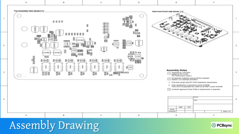
What’s the difference between a fabrication drawing and an assembly drawing?
A fabrication drawing tells the PCB manufacturer how to build the bare board—it includes layer stackup, drill chart, material specifications, and board dimensions. An assembly drawing tells the contract manufacturer how to populate that board with components—it shows component locations, reference designators, and polarity markings. These are separate documents for separate vendors, though some designers combine basic information onto shared drawing sheets.
Do I need a fabrication drawing if I’m using an online PCB service?
Online PCB services like JLCPCB or PCBWay capture most specifications through their web interface, reducing the need for a traditional fab drawing. However, including a fab drawing with your order ensures your requirements are documented and provides a reference if questions arise. For anything beyond standard capabilities—controlled impedance, special materials, tight tolerances—a fab drawing becomes essential even with online services.
Which IPC class should I specify in my fab notes?
IPC-6012 Class 2 is appropriate for most commercial and industrial electronics. It provides good reliability without excessive cost. Class 3 is for high-reliability applications (medical, aerospace, military) where failure has serious consequences. Class 1 is for general consumer products where cosmetic imperfections are acceptable. When in doubt, Class 2 is the safe default that balances quality and cost.
How detailed should my layer stackup be?
For two-layer boards, specifying the finished thickness in your fab notes is usually sufficient. For four or more layers, include a detailed stackup drawing showing layer order, copper weights, dielectric materials, and thicknesses. For controlled impedance designs, the stackup must show dielectric constants and the specific layers involved in impedance calculations. Let the manufacturer optimize prepreg and core combinations unless you have specific requirements.
Should I specify the exact drill sizes or let the manufacturer optimize?
Specify finished hole sizes in your drill chart and let the manufacturer select appropriate drill bit sizes to achieve those dimensions after plating. Manufacturers account for plating thickness (typically 0.001″ on each wall) when selecting drill bits. The exception is non-plated holes, where you should specify the actual drill size since no plating will be added.
Conclusion
A well-crafted fabrication drawing transforms your PCB design data into clear manufacturing instructions. It eliminates assumptions, prevents errors, and ensures your boards get built to your exact specifications. The time invested in creating complete fab documentation pays dividends in faster turnaround, fewer engineering questions, and higher-quality finished products.
Start with the essential elements—board outline, drill chart, stackup, and fab notes—then add detail based on your design’s complexity. Reference IPC standards rather than restating them, be specific about anything non-standard, and verify consistency between your fab drawing and your Gerber data.
Your fabricator will thank you, and your boards will arrive exactly as you designed them.
Inquire: Call 0086-755-23203480, or reach out via the form below/your sales contact to discuss our design, manufacturing, and assembly capabilities.
Quote: Email your PCB files to Sales@pcbsync.com (Preferred for large files) or submit online. We will contact you promptly. Please ensure your email is correct.
Notes: For PCB fabrication, we require PCB design file in Gerber RS-274X format (most preferred), *.PCB/DDB (Protel, inform your program version) format or *.BRD (Eagle) format. For PCB assembly, we require PCB design file in above mentioned format, drilling file and BOM. Click to download BOM template To avoid file missing, please include all files into one folder and compress it into .zip or .rar format.


