Inquire: Call 0086-755-23203480, or reach out via the form below/your sales contact to discuss our design, manufacturing, and assembly capabilities.
Quote: Email your PCB files to Sales@pcbsync.com (Preferred for large files) or submit online. We will contact you promptly. Please ensure your email is correct.
Notes: For PCB fabrication, we require PCB design file in Gerber RS-274X format (most preferred), *.PCB/DDB (Protel, inform your program version) format or *.BRD (Eagle) format. For PCB assembly, we require PCB design file in above mentioned format, drilling file and BOM. Click to download BOM template To avoid file missing, please include all files into one folder and compress it into .zip or .rar format.
The conversation I remember most vividly from my early career happened over a rejected prototype. Our team had designed a 6-layer multilayer flex PCB for a wearable heart monitor, confident it was the right choice. Manufacturing came back with yield rates below 60%, costs triple our budget, and bend radius performance that couldn’t meet spec. The redesign—a carefully optimized 4-layer construction—hit every target. That experience taught me something I’ve applied to every project since: choosing the right layer count for a multilayer flex PCB isn’t about maximizing capability. It’s about finding the precise configuration that meets your requirements without crossing into unnecessary complexity.
This guide will help you navigate that decision, covering when each layer count makes sense, how to evaluate your routing needs, and what trade-offs to consider between flexibility, cost, and performance.
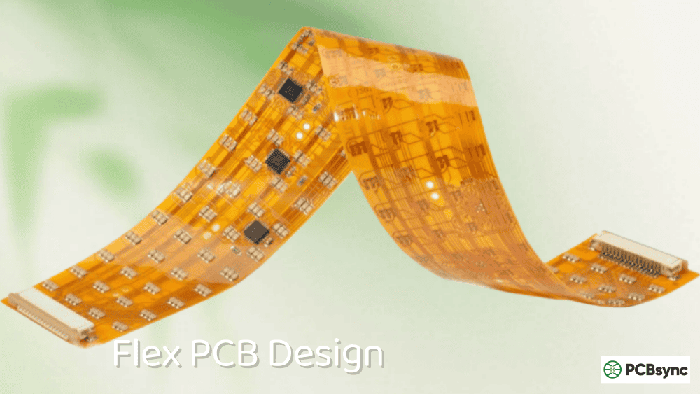
A multilayer flex PCB is a flexible printed circuit board containing three or more conductive copper layers separated by flexible dielectric materials, typically polyimide, and interconnected through plated through-holes, blind vias, or buried vias. Unlike single or double-sided flex circuits, multilayer flex PCB provides multiple routing channels, dedicated ground and power planes, and the capability to implement complex signal routing strategies while maintaining the ability to bend, fold, and conform to three-dimensional spaces.
The layer count in a multilayer flex PCB directly impacts nearly every aspect of the design: routing density, signal integrity, EMI performance, total thickness, bend radius capability, manufacturing complexity, and cost. Selecting the optimal layer count requires balancing these factors against your specific application requirements—a decision that affects project success from prototype through production.
How Multilayer Flex PCB Differs from Rigid Multilayer Boards
While multilayer flex PCB shares conceptual similarities with rigid multilayer construction, critical differences affect design decisions:
Limitations: Limited routing flexibility; ground/power plane must be shared; asymmetric construction can create warping challenges.
4-Layer Flex PCB Configuration
The 4-layer multilayer flex PCB is the most common configuration for applications requiring dedicated ground and power planes while maintaining good flexibility.
Typical stack-up: Signal / Ground / Power / Signal
Best applications:
High-speed digital interfaces requiring controlled impedance
Medical imaging and telecommunications applications
Considerations: Reduced flexibility compared to 4-layer; significantly increased cost; longer lead times; manufacturer capability verification required.
8-Layer and Higher Flex PCB Configurations
Eight-layer and higher multilayer flex PCB represents the upper practical limit for pure flexible circuits, reserved for the most demanding applications.
Best applications:
Extreme routing density requirements
Maximum EMI shielding for sensitive RF circuits
High channel-count systems (medical imaging, phased arrays)
Aerospace and defense applications with strict performance requirements
Considerations: Limited flexibility; significant cost premium; few manufacturers capable; often better served by rigid-flex construction.
Key Factors for Choosing Multilayer Flex PCB Layer Count
Selecting the right layer count requires systematic evaluation of multiple factors. Here’s the framework I use for every project:
Factor 1: Routing Density Requirements
The most fundamental driver of layer count is whether your design can be routed on available layers.
Component Type
Estimated Routing Layers Needed
Through-hole connectors
1-2 layers
0.5mm pitch QFP
2 layers
0.5mm pitch BGA (≤100 balls)
2-3 layers
0.4mm pitch BGA (100-300 balls)
3-4 layers
0.4mm pitch BGA (>300 balls)
4-6 layers
0.35mm pitch BGA
4-6+ layers (HDI required)
Practical approach: Use your EDA tool’s routing density analysis before finalizing layer count. Route the most constrained portion of your design first to validate layer assumptions.
Factor 2: Signal Integrity Requirements
High-speed signals and controlled impedance requirements often mandate specific layer configurations:
Signal Type
Minimum Layer Configuration
Low-speed digital (<50 MHz)
2 layers adequate
Moderate speed (50-200 MHz)
3-4 layers (microstrip)
High-speed (200 MHz – 1 GHz)
4 layers (ground reference)
Very high-speed (>1 GHz)
4-6 layers (stripline preferred)
Differential pairs (USB, LVDS)
4+ layers (controlled impedance)
RF signals
4-6 layers (shielding required)
For controlled impedance requirements, remember that each signal layer needs an adjacent reference plane. A 4-layer multilayer flex PCB with Signal/Ground/Power/Signal supports microstrip on both outer layers, while 6-layer construction enables internal stripline routing with superior EMI performance.
Factor 3: Power Distribution Needs
Complex power requirements can drive layer count independent of routing needs:
This is where multilayer flex PCB diverges most dramatically from rigid board decisions. More layers mean more material, which directly reduces flexibility:
Layer Count
Typical Thickness
Static Bend Radius
Dynamic Bend Radius
2-layer
0.1-0.15 mm
0.6-1.0 mm
1.5-3.0 mm
3-layer
0.15-0.20 mm
1.0-1.5 mm
2.5-4.0 mm
4-layer
0.20-0.35 mm
1.5-2.5 mm
4.0-7.0 mm
6-layer
0.30-0.50 mm
2.5-4.0 mm
7.0-12.0 mm
8-layer
0.45-0.70 mm
4.0-6.0 mm
12.0-18.0 mm
Critical question: What bend radius does your application actually require? Many designs specify tighter bends than necessary, driving layer count decisions that could be relaxed with proper mechanical analysis.
These multipliers compound with other factors like blind/buried vias, tight tolerances, and small features. A 6-layer multilayer flex PCB with HDI features can cost 5-8× more than a 2-layer design.
Layer Count Decision Framework for Multilayer Flex PCB
Based on the factors above, here’s a systematic approach to selecting your layer count:
Step 1: Establish Minimum Viable Layer Count
Start by determining the absolute minimum layers your design requires:
Routing minimum: Analyze your most constrained area (typically BGA escape routing). If routing completes on N signal layers, you need N signal layers plus required planes.
Signal integrity minimum: Identify your highest-speed signals. Do they require adjacent reference planes? Stripline configuration?
Power minimum: Count distinct power domains requiring isolation. Each isolated domain may need dedicated plane area.
Your minimum layer count = Maximum of (routing, signal integrity, power requirements)
Step 2: Validate Against Flexibility Requirements
With your minimum layer count established:
Calculate expected total thickness based on your layer count and materials
Determine resulting minimum bend radius (typically 6-10× thickness for static, 15-25× for dynamic)
Compare against your actual application bend requirements
If bend radius is acceptable, proceed. If not, consider:
Reducing layer count in flex regions (rigid-flex approach)
Using thinner materials (adhesiveless construction)
Reducing copper weight
Relaxing bend requirements if possible
Step 3: Apply Cost-Benefit Analysis
Before finalizing, evaluate whether design optimization could reduce layer count:
Optimization Strategy
Potential Layer Reduction
Routing optimization
1 layer
Component selection (larger pitch)
1-2 layers
Design partitioning (rigid-flex)
2+ layers in flex region
Hatched ground planes
Can enable fewer layers
HDI technology adoption
May allow fewer layers
The goal is finding the lowest layer count that reliably meets all requirements with appropriate manufacturing margin.
Multilayer Flex PCB Stack-Up Design by Layer Count
Once you’ve selected your layer count, proper stack-up design ensures optimal performance.
Frequently Asked Questions About Multilayer Flex PCB Layer Count
How do I know if my design needs a multilayer flex PCB versus double-sided?
Your design likely needs a multilayer flex PCB when it includes any of the following: fine-pitch BGAs with pitches below 0.5mm that require escape routing beyond two layers, high-speed signals above 200MHz requiring controlled impedance with dedicated reference planes, complex power distribution with multiple isolated voltage domains, or EMI-sensitive circuits requiring shielding planes. A practical test: attempt routing on a double-sided design. If routing completion falls below 90% with acceptable trace lengths, or if signal integrity analysis shows unacceptable performance, multilayer construction is warranted. For borderline cases, the cost premium for a 3 or 4-layer multilayer flex PCB often provides insurance against routing challenges that emerge during detailed design.
What is the maximum practical layer count for a flexible circuit that still bends?
For circuits requiring meaningful flexibility, 6 layers represents a practical upper limit for most applications, yielding total thickness around 0.3-0.5mm with minimum bend radii of 2.5-4.0mm for static installation. Eight-layer multilayer flex PCB can achieve bend radii of 4-6mm, suitable for flex-to-install applications but generally too stiff for dynamic flexing. For designs requiring more than 6 layers with tight bend requirements, rigid-flex construction typically provides better results—using fewer layers in flex regions while achieving higher counts in rigid sections. Some specialized applications achieve 10-12 layer flex using bookbinding techniques that separate layers in bend zones, but these require specialized manufacturers and significant cost premiums.
How does layer count affect lead time for multilayer flex PCB?
Each additional layer pair adds manufacturing complexity and time. Typical lead times by layer count are: 2-layer (7-10 days prototype), 3-4 layer (10-15 days prototype), 6-layer (15-25 days prototype), and 8-layer (25-40 days prototype). The extended time reflects additional lamination cycles, more process steps, and increased inspection requirements. Production quantities typically require 2-4 weeks for 4-layer, 4-6 weeks for 6-layer, and 6-10 weeks for 8-layer designs. Rush services can reduce these timelines by 30-50% at premium pricing, but fundamental process constraints prevent dramatic acceleration. Plan your project timeline based on realistic layer count lead times.
Can I use different layer counts in different regions of a flex circuit?
Yes, through rigid-flex construction, which combines flexible and rigid sections in a single integrated assembly. In a rigid-flex design, flexible regions can use 2-4 layers while rigid sections can incorporate 6, 8, or more layers for dense component mounting and complex routing. This approach often provides superior overall results compared to forcing high layer counts throughout a pure flex design—maintaining flexibility where needed while achieving routing density in rigid sections. The transition between rigid and flex regions requires careful design attention, but rigid-flex is frequently the optimal solution for complex applications that might otherwise demand 6+ layer pure flex construction.
What’s the cost difference between 4-layer and 6-layer multilayer flex PCB?
A 6-layer multilayer flex PCB typically costs 40-70% more than an equivalent 4-layer design, with exact premiums depending on complexity, volume, and manufacturer. For example, a 100×50mm 4-layer flex might cost $400-800 for prototype quantities, while the same design in 6-layer could run $600-1,400. At production volumes (1,000+ units), per-unit costs might be $2-4 for 4-layer versus $3.50-6 for 6-layer. Beyond direct layer cost, 6-layer designs often require tighter tolerances, more complex via structures, and longer manufacturing times that compound the premium. Before committing to 6 layers, verify through routing analysis that the additional layers are genuinely necessary, as optimization sometimes allows 4-layer implementation at substantial cost savings.
Useful Resources for Multilayer Flex PCB Design
Industry Standards
IPC-6013: Qualification and Performance Specification for Flexible/Rigid-Flexible Printed Boards
IPC-2223: Sectional Design Standard for Flexible Printed Boards
Choosing the right layer count for your multilayer flex PCB comes down to honest assessment of your requirements combined with systematic evaluation of trade-offs. The optimal configuration is the lowest layer count that reliably meets your routing, signal integrity, power distribution, and flexibility requirements—with appropriate margin for manufacturing variation and design evolution.
That heart monitor project I mentioned taught me that more layers don’t automatically mean better design. The 4-layer solution that replaced our failed 6-layer attempt performed better in every metric that mattered: better flexibility, higher manufacturing yield, lower cost, and faster delivery. The key was understanding what our application actually required rather than what we assumed it needed.
Apply the framework in this guide, validate assumptions through analysis, and engage your manufacturer early in the process. The right layer count decision made early in your project sets the foundation for success from prototype through production.
Inquire: Call 0086-755-23203480, or reach out via the form below/your sales contact to discuss our design, manufacturing, and assembly capabilities.
Quote: Email your PCB files to Sales@pcbsync.com (Preferred for large files) or submit online. We will contact you promptly. Please ensure your email is correct.
Notes: For PCB fabrication, we require PCB design file in Gerber RS-274X format (most preferred), *.PCB/DDB (Protel, inform your program version) format or *.BRD (Eagle) format. For PCB assembly, we require PCB design file in above mentioned format, drilling file and BOM. Click to download BOM template To avoid file missing, please include all files into one folder and compress it into .zip or .rar format.


