Inquire: Call 0086-755-23203480, or reach out via the form below/your sales contact to discuss our design, manufacturing, and assembly capabilities.
Quote: Email your PCB files to Sales@pcbsync.com (Preferred for large files) or submit online. We will contact you promptly. Please ensure your email is correct.
Notes: For PCB fabrication, we require PCB design file in Gerber RS-274X format (most preferred), *.PCB/DDB (Protel, inform your program version) format or *.BRD (Eagle) format. For PCB assembly, we require PCB design file in above mentioned format, drilling file and BOM. Click to download BOM template To avoid file missing, please include all files into one folder and compress it into .zip or .rar format.
The project that changed how I think about flexible circuits came from a medical device startup three years ago. They needed to fit a 12-lead ECG monitoring system into a chest patch smaller than a credit card—with Bluetooth connectivity, signal processing, and three days of battery life. Traditional flex circuits couldn’t route the 0.4mm pitch BGA processor. Standard HDI boards were too rigid for body contour. The answer was HDI flex PCB technology, and watching that first prototype capture clean cardiac waveforms while conforming to a patient’s chest showed me that this combination of high-density interconnect and flexible substrates represents the future of miniaturized electronics.
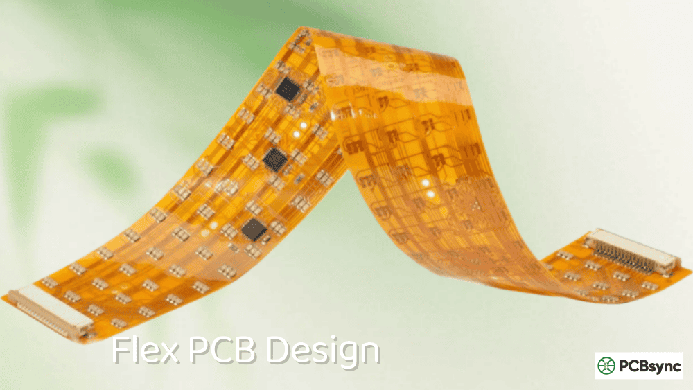
This guide covers the essential knowledge for successfully designing and manufacturing HDI flex PCB—from microvia fundamentals to critical design rules that ensure manufacturability.
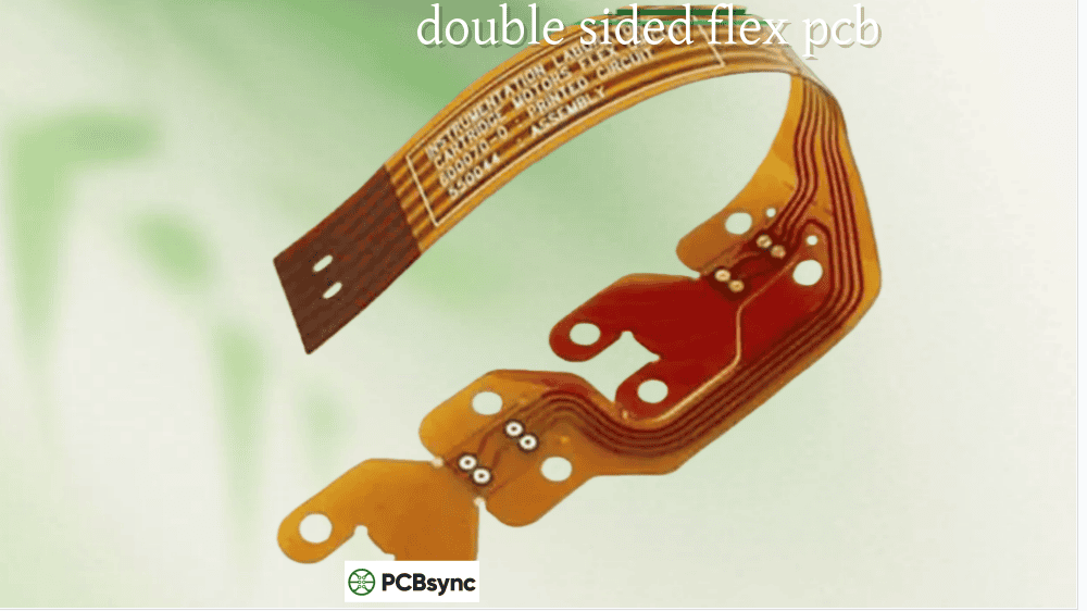
HDI flex PCB combines high-density interconnect technology with flexible printed circuit substrates, creating circuits that offer both exceptional routing density and the ability to bend, fold, or conform to complex shapes. Where traditional flex circuits might use 150-200μm trace widths and mechanical through-hole vias, HDI flex PCB incorporates microvias, fine lines below 100μm, and advanced layer structures that dramatically increase interconnect density while maintaining flexibility.
The IPC defines high-density interconnect boards as having one or more of the following characteristics: microvias with diameters of 150μm or less, trace widths and spacing below 100μm, capture pads under 400μm, and connection pad density exceeding 20 per square centimeter. When these HDI features are implemented on flexible polyimide substrates rather than rigid FR-4, the result is HDI flex PCB—a technology that enables the most demanding miniaturization applications in modern electronics.
Why HDI Flex PCB Matters for Modern Electronics
The convergence of several industry trends has made HDI flex PCB increasingly essential:
Component miniaturization: Modern ICs use ball pitches as fine as 0.3-0.4mm, requiring microvia technology for escape routing that traditional flex circuits cannot achieve.
Device form factors: Wearables, implantables, and IoT devices demand circuits that fit curved surfaces and tight enclosures while supporting complex functionality.
Signal integrity: Higher operating frequencies require controlled impedance and shorter signal paths that HDI architectures provide.
Reliability requirements: Eliminating connectors and cable assemblies through integrated flex sections reduces failure points in mission-critical applications.
Microvia Technology in HDI Flex PCB
Microvias are the defining feature that distinguishes HDI flex PCB from conventional flexible circuits. These laser-drilled interconnects enable the routing density that makes modern fine-pitch component packaging possible.
Understanding Microvia Types for HDI Flex PCB
Microvia Type
Description
Typical Diameter
Best Application
Blind microvia
Connects outer layer to adjacent inner layer
75-150 μm
BGA fan-out routing
Buried microvia
Connects inner layers only
75-150 μm
Internal layer connections
Stacked microvia
Multiple microvias aligned vertically
75-100 μm
Maximum density designs
Staggered microvia
Offset microvias on successive layers
75-150 μm
Better reliability, lower cost
Via-in-pad (VIP)
Microvia placed directly in component pad
75-100 μm
Ultra-fine pitch BGAs
Microvia Design Rules for HDI Flex PCB
Proper microvia design is critical for HDI flex PCB reliability. These parameters ensure manufacturable, reliable interconnects:
The choice between stacked and staggered microvia configurations significantly impacts both performance and manufacturability:
Factor
Stacked Microvias
Staggered Microvias
Routing density
Maximum
High
Signal path length
Shortest
Slightly longer
Manufacturing complexity
Higher
Lower
Reliability
Good with proper fill
Excellent
Cost
20-40% premium
Standard HDI pricing
Thermal cycling performance
Stress concentration risk
Better stress distribution
Recommended use
Ultra-dense designs
Most HDI flex PCB applications
For most HDI flex PCB designs, staggered microvias offer the best balance of density, reliability, and cost. Reserve stacked configurations for applications where routing density absolutely requires vertical via alignment.
Successful HDI flex PCB design requires adherence to tighter tolerances than conventional flexible circuits. These rules ensure your design is manufacturable while achieving the density benefits HDI technology offers.
Trace and Space Requirements for HDI Flex PCB
Design Parameter
Standard HDI Flex
Advanced HDI Flex
Ultra-HDI Flex
Minimum trace width
75 μm (3 mil)
50 μm (2 mil)
25-38 μm (1-1.5 mil)
Minimum spacing
75 μm (3 mil)
50 μm (2 mil)
25-38 μm (1-1.5 mil)
Copper thickness
12-18 μm (⅓-½ oz)
9-12 μm (¼-⅓ oz)
5-9 μm (⅛-¼ oz)
Impedance tolerance
±10%
±7%
±5%
Registration accuracy
±50 μm
±37.5 μm
±25 μm
HDI Flex PCB Layer Configurations
HDI structures are described using the notation X+N+X, where X represents the number of sequential build-up layers on each side and N represents the core layer count:
Configuration
Structure
Total Layers
Typical Application
1+N+1
1 build-up each side + core
4-6 layers
Standard HDI flex PCB
2+N+2
2 build-ups each side + core
6-8 layers
High-density designs
3+N+3
3 build-ups each side + core
8-10 layers
Maximum density
ELIC
Every layer interconnect
4-8+ layers
Ultra-high density
For HDI flex PCB, 1+N+1 and 2+N+2 configurations are most common, balancing density requirements with the flexibility characteristics that make the technology valuable.
Critical Design Considerations for HDI Flex PCB
Component placement: Position fine-pitch BGAs and other high-density components in rigid or stiffened areas where microvia structures can be optimally supported. Avoid placing components that require via-in-pad in dynamic flex zones.
Routing strategies: Use microvias for BGA escape routing, transitioning to standard traces for longer runs. Route perpendicular to bend lines in flex zones, and keep HDI structures away from areas requiring repeated flexing.
Copper balance: Maintain copper distribution within 15% between layers to prevent warping during lamination. This becomes more challenging with fine-line HDI features and requires careful planning.
Flex zone design: Minimize or eliminate microvias in dynamic flex regions. When microvias must exist near flex zones, maintain minimum 1.5mm clearance from bend lines and use staggered rather than stacked configurations.
Miniaturization Advantages of HDI Flex PCB
The primary driver for HDI flex PCB adoption is miniaturization—achieving more functionality in less space. The technology delivers this through multiple mechanisms.
Size and Weight Reduction with HDI Flex PCB
Benefit
Typical Improvement
How It’s Achieved
Board area reduction
30-50%
Finer traces, higher routing density
Layer count reduction
1-2 fewer layers
More efficient routing per layer
Thickness reduction
20-40%
Thinner dielectrics, fewer layers
Weight reduction
25-50%
Less material, integrated connections
Component density
2-3× increase
Via-in-pad, fine-pitch support
Interconnect elimination
Up to 100%
Integrated flex replaces cables
A practical example: an 8-layer standard flex PCB design can often be implemented as a 6-layer HDI flex PCB with equivalent or better routing capacity, reducing both thickness and weight while improving signal integrity.
Shorter signal paths: Microvias and via-in-pad technology reduce routing lengths by 25-40% compared to dog-bone fan-out patterns, directly improving signal integrity at high frequencies.
Reduced parasitic effects: Smaller via structures have lower parasitic capacitance and inductance. A 100μm microvia presents approximately 0.3pF capacitance versus 0.7-1.0pF for standard through-hole vias.
Better impedance control: Fine-line HDI enables precise impedance matching with tolerances of ±5-7%, supporting controlled impedance requirements for high-speed differential signaling.
Enhanced EMI performance: Higher routing density with proper ground plane integration provides superior electromagnetic shielding, achieving 15-20dB better EMI suppression than equivalent conventional designs.
HDI Flex PCB Manufacturing Process
Manufacturing HDI flex PCB requires specialized capabilities beyond standard flex circuit production. Understanding the process helps designers create more manufacturable designs.
HDI flex PCB commands premium pricing compared to conventional flexible circuits, but the value proposition often favors HDI when total system cost is considered.
Cost Comparison
Specification
Standard Flex
HDI Flex PCB
Cost Driver
Base cost multiplier
1×
2-4×
Laser drilling, sequential lamination
Prototype (100×100mm)
$200-600
$500-2,000
Process complexity
Production per dm²
$80-200
$200-600
Yield, equipment utilization
Lead time (prototype)
10-15 days
15-25 days
Additional process steps
Lead time (production)
3-4 weeks
4-6 weeks
Sequential build-up cycles
When HDI Flex PCB Provides Value
Despite higher board costs, HDI flex PCB often reduces total system cost:
Layer reduction: Achieving equivalent routing in fewer layers can offset HDI process costs while reducing thickness and weight.
Connector elimination: Each eliminated connector saves $0.50-5.00 in component cost plus assembly labor, while improving reliability.
Size-driven value: In space-constrained applications, the premium for HDI flex PCB may be insignificant compared to the value of achieving required form factors.
Yield improvement: Better signal integrity and fewer interconnects can improve system-level manufacturing yield, offsetting board cost premiums.
Frequently Asked Questions About HDI Flex PCB
What is the difference between HDI flex PCB and standard flexible circuits?
HDI flex PCB incorporates high-density interconnect features—primarily laser-drilled microvias (≤150μm diameter), fine traces below 100μm, and advanced build-up layer structures—on flexible polyimide substrates. Standard flexible circuits use conventional mechanical drilling (minimum ~200μm), wider traces (typically 100-150μm minimum), and simpler layer structures. The result is that HDI flex PCB achieves 2-3× higher interconnect density while maintaining flexibility, enabling support for fine-pitch components (0.3-0.5mm BGA pitch) that standard flex cannot accommodate.
Can HDI flex PCB be used in dynamic flexing applications?
Yes, but with important constraints. HDI flex PCB can handle dynamic flexing when microvias and fine-pitch components are located in static regions, with standard flex construction used in dynamic bend zones. For applications requiring repeated flexing, design the circuit so HDI structures remain in rigid or semi-rigid areas, using rolled annealed copper and staggered (not stacked) microvias where vias must exist near flex regions. With proper design, HDI flex PCB can achieve 100,000+ flex cycles in hybrid configurations, though pure dynamic flex zones should minimize or eliminate microvia structures.
What is the minimum bend radius for HDI flex PCB?
Minimum bend radius for HDI flex PCB depends on total thickness and construction. For static (flex-to-install) applications, use 6-10× total thickness in standard flex areas and 10-15× in regions containing HDI structures. For dynamic flexing, increase to 15-25× thickness in flex zones. A typical 4-layer HDI flex PCB with 0.2mm total thickness requires approximately 2-3mm bend radius for static installation. Keep HDI features—particularly stacked microvias and via-in-pad structures—at least 1.5mm away from bend centerlines to prevent stress-induced failures.
How does HDI flex PCB affect signal integrity compared to standard flex?
HDI flex PCB significantly improves signal integrity through multiple mechanisms. Microvias reduce parasitic capacitance by 50-70% compared to through-hole vias (0.3pF vs 0.7-1.0pF typical), minimizing signal reflections. Shorter routing paths from via-in-pad technology reduce signal propagation delays and losses. Fine-line capability enables precise impedance control (±5-7% vs ±10% for standard flex), critical for high-speed differential pairs. The ability to implement proper ground planes adjacent to signal layers provides better EMI shielding and reference plane integrity. These improvements support data rates exceeding 10Gbps when properly designed.
What are the typical lead times for HDI flex PCB prototypes?
HDI flex PCB prototypes typically require 15-25 business days, compared to 10-15 days for standard flexible circuits. The extended timeline reflects additional laser drilling operations, sequential lamination cycles (each adding 2-3 days), microvia plating and fill processes, and more extensive electrical testing. Premium expedited services can reduce prototype lead times to 10-15 days at significant cost premiums (often 50-100% of base price). For production quantities, plan for 4-6 weeks versus 3-4 weeks for standard flex. Complex designs with multiple build-up layers (2+N+2 or higher) or ultra-fine features may require additional time.
Useful Resources for HDI Flex PCB Design
Industry Standards
IPC-2226: Sectional Design Standard for High Density Interconnect (HDI) Printed Boards
IPC-6013: Qualification and Performance Specification for Flexible/Rigid-Flexible Printed Boards
IPC-6016: Qualification and Performance Specification for HDI Structures
IPC-4104: Specification for High Density Interconnect (HDI) and Microvia Materials
IPC-TM-650: Test Methods Manual (microvia reliability testing)
Design Software
Altium Designer: www.altium.com – HDI design rules and microvia support
HDI flex PCB represents the convergence of two powerful PCB technologies—delivering the routing density and fine-pitch component support of high-density interconnect along with the form factor flexibility that enables next-generation miniaturized electronics. The technology excels when designs require:
Support for 0.3-0.5mm pitch BGA packages in flexible circuits
Maximum functionality in minimum volume
Integration of rigid-mount components with flexible interconnects
High-speed signal integrity in compact, conformable form factors
Elimination of connectors and cables in reliability-critical applications
The medical ECG patch I mentioned at the start has now completed clinical trials and is heading toward FDA clearance. That success came from understanding when HDI flex PCB technology was truly necessary—and equally important, understanding the design rules and manufacturing constraints that ensure reliable production. Master those fundamentals, and HDI flex PCB becomes a powerful tool for creating electronics that simply weren’t possible a decade ago.
Inquire: Call 0086-755-23203480, or reach out via the form below/your sales contact to discuss our design, manufacturing, and assembly capabilities.
Quote: Email your PCB files to Sales@pcbsync.com (Preferred for large files) or submit online. We will contact you promptly. Please ensure your email is correct.
Notes: For PCB fabrication, we require PCB design file in Gerber RS-274X format (most preferred), *.PCB/DDB (Protel, inform your program version) format or *.BRD (Eagle) format. For PCB assembly, we require PCB design file in above mentioned format, drilling file and BOM. Click to download BOM template To avoid file missing, please include all files into one folder and compress it into .zip or .rar format.


