Inquire: Call 0086-755-23203480, or reach out via the form below/your sales contact to discuss our design, manufacturing, and assembly capabilities.
Quote: Email your PCB files to Sales@pcbsync.com (Preferred for large files) or submit online. We will contact you promptly. Please ensure your email is correct.
Notes: For PCB fabrication, we require PCB design file in Gerber RS-274X format (most preferred), *.PCB/DDB (Protel, inform your program version) format or *.BRD (Eagle) format. For PCB assembly, we require PCB design file in above mentioned format, drilling file and BOM. Click to download BOM template To avoid file missing, please include all files into one folder and compress it into .zip or .rar format.
When our aerospace client came to us with a radar system redesign, the constraints seemed almost impossible. They needed to route over 200 high-speed differential pairs through a circuit that would fold into a cylindrical antenna assembly, survive temperature cycling from -55°C to +125°C, and maintain signal integrity at 10GHz. Six-layer flex couldn’t provide the routing density. Rigid-flex would have added unacceptable weight. The solution was 8 layer flex PCB—and watching that design perform flawlessly in qualification testing confirmed what I’d suspected: when applications demand the absolute pinnacle of flexible circuit capability, eight layers deliver what nothing else can.
This guide explores when 8 layer flex PCB becomes the right choice, how to design these complex circuits successfully, and what to expect from the manufacturing process.
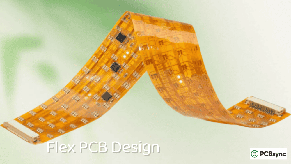
An 8 layer flex PCB is a flexible printed circuit board containing eight conductive copper layers separated by flexible dielectric materials, typically polyimide. These layers are interconnected through plated through-holes, blind vias, buried vias, and microvias to create the highest-density interconnect structures available in flexible circuit technology while maintaining the ability to bend and conform to complex shapes.
Eight-layer flex represents the practical limit for most pure flexible circuit applications. Beyond this layer count, the accumulated thickness typically compromises flexibility to the point where rigid-flex construction becomes more appropriate. Within this eight-layer envelope, designers gain extraordinary routing density, multiple dedicated ground and power planes, comprehensive EMI shielding, and the signal integrity performance required for the most demanding high-speed applications.
The 8 layer flex PCB occupies a specialized niche—applications where six layers can’t deliver sufficient routing capacity or signal isolation, where rigid-flex isn’t appropriate due to weight, size, or continuous flexibility requirements, and where the substantial cost premium is justified by performance demands that no simpler solution can meet.
When to Choose 8 Layer Flex PCB
Selecting 8 layer flex PCB represents a significant engineering and financial commitment. Here’s when it makes sense:
Extreme Routing Density Requirements
When your design includes multiple fine-pitch BGAs, hundreds of I/O connections, or complex mixed-signal circuits that exhaust six-layer routing capacity, 8 layer flex PCB provides the additional channels needed. The two extra layers can increase routing capacity by 30-50% compared to six-layer designs.
Maximum Signal Integrity Performance
Eight layers enable optimal signal-ground-signal-ground-power-ground-signal-signal configurations where critical signals have dedicated adjacent reference planes with additional isolation layers. This architecture minimizes crosstalk to levels unachievable with fewer layers and supports controlled impedance at frequencies exceeding 10GHz.
Complete EMI Shielding Requirements
Applications requiring electromagnetic compatibility in demanding RF environments benefit from 8 layer flex PCB’s ability to provide multiple shielding planes. Complete signal encapsulation between ground planes achieves 15-20dB additional EMI suppression compared to four-layer designs.
Complex Power Distribution Needs
Designs requiring multiple isolated power domains, numerous voltage rails, or high-current distribution alongside sensitive analog circuits need the dedicated plane layers that only eight-layer construction provides while maintaining flexibility.
High Channel Count Systems
Medical imaging, telecommunications, and data acquisition systems with hundreds of signal channels often require 8 layer flex PCB to achieve necessary routing density while maintaining signal quality and isolation between channels.
8 Layer Flex PCB Stack-Up Design
Stack-up configuration is critical for 8 layer flex PCB performance. The arrangement of signal, ground, and power layers determines signal integrity, EMI performance, and manufacturing success.
This configuration provides optimal balance of routing capacity, signal integrity, and EMI performance:
Layer
Function
Material
Typical Thickness
Reference
Coverlay
Protection
PI + adhesive
25-37.5 μm
—
L1
High-speed signals
RA copper
9-18 μm (¼-½ oz)
L2 (GND)
Dielectric 1
Insulation
Polyimide
25-50 μm
—
L2
Ground plane
RA copper
9-18 μm
—
Core 1
Structural
Polyimide
37.5-50 μm
—
L3
Internal signals
RA copper
9-18 μm
L2/L4
Dielectric 2
Insulation
Polyimide
25-37.5 μm
—
L4
Power plane
RA copper
9-18 μm
—
Core 2
Central core
Polyimide
50-75 μm
—
L5
Ground plane
RA copper
9-18 μm
—
Dielectric 3
Insulation
Polyimide
25-37.5 μm
—
L6
Internal signals
RA copper
9-18 μm
L5/L7
Core 3
Structural
Polyimide
37.5-50 μm
—
L7
Ground plane
RA copper
9-18 μm
—
Dielectric 4
Insulation
Polyimide
25-50 μm
—
L8
High-speed signals
RA copper
9-18 μm (¼-½ oz)
L7 (GND)
Coverlay
Protection
PI + adhesive
25-37.5 μm
—
Total thickness for a typical 8 layer flex PCB ranges from 0.4mm to 1.0mm depending on materials and design requirements.
Why This Stack-Up Works
Optimal signal referencing: Outer signal layers (L1, L8) have immediately adjacent ground planes (L2, L7) for best impedance control and EMI performance. Inner signal layers (L3, L6) are sandwiched between planes for complete shielding.
Power integrity: The L4 power plane paired with adjacent ground planes (L5 above, L2 below through capacitive coupling) provides excellent power delivery and decoupling.
Symmetrical construction: The balanced arrangement prevents warping during manufacturing and ensures uniform mechanical properties throughout the flex circuit.
EMI containment: Multiple ground planes create a Faraday cage effect around internal signals, achieving 15-20dB reduction in radiated emissions compared to four-layer constructions.
Design Guidelines for 8 Layer Flex PCB
Designing 8 layer flex PCB requires rigorous attention to constraints that become increasingly critical with higher layer counts.
Trace Routing Requirements
Parameter
Recommended Value
Notes
Minimum trace width
50-75 μm (2-3 mils)
HDI processes enable finer
Minimum spacing
50-75 μm (2-3 mils)
Match to trace width
High-speed routing
Outer layers (L1, L8)
Best reference planes
Sensitive analog
Inner layers (L3, L6)
Maximum shielding
Adjacent layer routing
Perpendicular orientation
Minimizes crosstalk
Via-to-bend distance
>2.5mm (100 mils)
Critical for reliability
Copper balance
Within 15% per side
Prevents warping
Bend Radius Requirements for 8 Layer Flex PCB
The substantial thickness of 8 layer flex PCB demands generous bend radii:
Application
Minimum Bend Radius
Example (0.6mm thickness)
Static (flex-to-install)
12-15× total thickness
7.2-9.0mm
Dynamic (limited cycles)
25-35× total thickness
15.0-21.0mm
Dynamic (high cycles)
40-50× total thickness
24.0-30.0mm
These requirements significantly exceed those for simpler flex constructions. For applications requiring tight bend radii, consider rigid-flex construction where flexible sections use fewer layers.
Via Strategy for 8 Layer Flex PCB
Via Type
Layer Connections
Advantages
Best Use
Through-hole
All 8 layers
Simple process
Static regions only
Blind (L1-L2)
Outer to first inner
Preserves flexibility
Component escape routing
Blind (L7-L8)
Outer to last inner
Preserves flexibility
Component escape routing
Buried (L2-L7)
Inner layers only
Hidden from stress
Inner layer connections
Buried (L3-L6)
Middle layers
Minimal flex impact
Internal routing
Stacked microvia
Sequential pairs
Maximum density
HDI requirements
For 8 layer flex PCB, strategic via planning is essential. Minimize through-holes in flex zones—they create the greatest stress concentration. Use blind and buried vias to maintain flexibility while achieving necessary layer connections.
Impedance Control in 8 Layer Flex PCB
Signal Type
Target Impedance
Stack-Up Consideration
Single-ended
50Ω typical
Route on L1/L8 over ground planes
Differential pairs
100Ω typical
Maintain consistent spacing
High-frequency (>5GHz)
Application-specific
Use low-loss polyimide
Controlled stripline
50Ω typical
Inner layers between planes
The multiple reference planes in 8 layer flex PCB enable impedance control accuracy within ±5%, meeting the requirements of high-frequency applications up to and beyond 10GHz.
Manufacturing 8 layer flex PCB requires the most advanced flex fabrication capabilities. The process involves multiple lamination cycles, precise layer registration, and specialized handling throughout.
Manufacturing Complexity
Factor
4 Layer Flex
6 Layer Flex
8 Layer Flex PCB
Lamination cycles
1-2
2-3
3-4
Registration tolerance
±75 μm
±50 μm
±37.5 μm
Process steps
~40
~55
~70+
Typical yield
90-95%
85-92%
75-88%
Quality inspection points
Standard
Enhanced
Comprehensive
Key Manufacturing Steps
Inner core fabrication: The process begins with fabricating inner layer pairs (L3-L4, L5-L6) on thin flex cores. These cores are drilled, plated, imaged, and etched independently.
First lamination: Inner cores are laminated with additional dielectric layers and copper foils to create intermediate assemblies.
Second lamination: The intermediate assemblies are laminated together with the central core, creating the six-inner-layer structure.
Final lamination: Outer copper layers (L1, L8) are laminated to complete the eight-layer stack.
Through-hole drilling and plating: Mechanical or laser drilling creates through-vias, followed by copper plating to establish layer-to-layer connections.
Outer layer imaging and etching: Circuit patterns are created on the outer layers.
Coverlay application: Polyimide coverlays are laminated over outer layers for protection.
Final processing: Surface finish, electrical testing, profiling, and inspection complete the process.
Manufacturer Qualification Requirements
Not all flex PCB fabricators can produce reliable 8 layer flex PCB. Essential capabilities include:
Capability
Requirement
Why It Matters
Layer count experience
Demonstrated 8+ layer flex
Process maturity
Registration accuracy
±37.5 μm or better
Via-to-pad reliability
Sequential lamination
Multiple cycle capability
Layer bonding quality
Microvia capability
Laser drilling, fill plating
HDI requirements
Impedance testing
TDR verification
High-speed performance
Cross-section analysis
In-house capability
Quality verification
IPC Class 3
Certified processes
High-reliability applications
Industry Applications for 8 Layer Flex PCB
The combination of maximum routing density, superior signal integrity, and maintained flexibility makes 8 layer flex PCB essential for the most demanding applications.
Eight-layer flex circuits represent the highest-cost tier of flexible PCB technology. Understanding cost drivers helps optimize designs and set appropriate budgets.
Cost Comparison by Layer Count
Specification
6 Layer Flex
8 Layer Flex PCB
Rigid-Flex 8L
Relative cost
1× (baseline)
1.8-2.5×
2.0-3.0×
Prototype cost
$800-2,000
$1,500-5,000+
$2,500-8,000+
Production cost/dm²
$250-600
$500-1,500+
$600-2,000+
Lead time (prototype)
15-25 days
25-40 days
30-50 days
Lead time (production)
4-6 weeks
6-10 weeks
8-12 weeks
Major Cost Drivers for 8 Layer Flex PCB
Factor
Cost Impact
Mitigation Strategy
Layer count
Primary driver
Verify 8 layers truly needed
Material selection
20-40% variation
Use standard polyimide where possible
Via complexity
15-30% for blind/buried
Minimize advanced via structures
Fine features
10-25% for HDI
Use standard trace/space when adequate
Surface finish
5-15% variation
Match finish to actual requirements
Panel utilization
10-20% variation
Optimize circuit layout for panelization
Testing requirements
5-15% for enhanced
Define appropriate test coverage
Cost Optimization Strategies
Rigorous layer count justification: Before committing to 8 layer flex PCB, conduct detailed routing analysis to confirm six layers cannot achieve design goals. The cost difference is substantial.
Strategic rigid-flex consideration: If portions of your design don’t require flexibility, rigid-flex construction may provide equivalent functionality at lower cost by using rigid (cheaper) sections where appropriate.
Standard material usage: Exotic low-loss dielectrics or unusual copper weights significantly increase cost. Use standard materials unless performance requirements mandate alternatives.
Via optimization: Each blind or buried via adds cost. Use through-holes where flexibility isn’t required, and design via structures to minimize manufacturing complexity.
Volume planning: 8 layer flex PCB shows stronger volume discounts than simpler constructions. If production quantities are planned, factor this into prototype-versus-production cost comparisons.
Frequently Asked Questions About 8 Layer Flex PCB
What is the typical thickness of an 8 layer flex PCB?
Standard 8 layer flex PCB thickness ranges from 0.4mm to 1.0mm. The specific value depends on copper weight (typically ¼-½ oz per layer for flexibility), dielectric thickness between layers (25-75 μm polyimide), and construction approach. Ultra-thin builds using ¼ oz copper and 25 μm dielectrics can approach 0.4mm, while designs requiring controlled impedance or heavier copper may reach 0.8-1.0mm. This thickness is substantially greater than 4-layer flex (0.2-0.4mm) or 6-layer flex (0.3-0.6mm), directly impacting minimum bend radius requirements.
Can 8 layer flex PCB handle dynamic flexing applications?
Yes, but with significant constraints. For dynamic flexing, use rolled annealed (RA) copper on all layers, adhesiveless construction where available, and maintain very generous bend radii (25-50× total thickness). Avoid placing any vias in flex zones, route all traces perpendicular to bend lines, and stagger traces between layers to distribute stress. Properly designed 8 layer flex PCB can achieve 1-10 million flex cycles depending on bend radius and material selection. For extreme flex cycle requirements exceeding 10 million cycles, consider reducing layer count in flex sections through rigid-flex construction.
How does 8 layer flex PCB compare to rigid-flex for complex applications?
Pure 8 layer flex PCB is appropriate when continuous flexibility throughout the circuit is required, when weight is absolutely critical (flex is lighter than equivalent rigid-flex), or when the form factor demands a uniformly thin, flexible construction. Rigid-flex becomes preferable when different sections need different layer counts, when significant component mounting requires rigid support, or when the total cost of rigid-flex is lower due to using simpler flex sections. For many high-layer-count applications, rigid-flex with 4-layer flex sections and 8-10 layer rigid sections provides better overall value than pure 8-layer flex.
What signal frequencies can 8 layer flex PCB support?
With proper design and materials, 8 layer flex PCB supports signal frequencies up to and beyond 10GHz. The multiple reference planes enable controlled impedance accuracy within ±5%, and the shielding capabilities minimize crosstalk at high frequencies. For frequencies above 6GHz, use low-loss polyimide materials and careful attention to via transitions. The stripline configurations available in 8-layer construction (signals completely enclosed between ground planes) provide superior high-frequency performance compared to microstrip structures on fewer-layer designs. Some specialized designs achieve acceptable performance at mmWave frequencies (28GHz+) with appropriate material selection.
What is the typical prototype lead time for 8 layer flex PCB?
Prototype lead times for 8 layer flex PCB typically run 25-40 business days, compared to 15-25 days for 6-layer flex. The extended timeline reflects multiple sequential lamination cycles, additional imaging/etching processes, more complex via structures, and comprehensive testing requirements. Premium expedited services may reduce this to 15-20 days at substantial cost premiums (often 100-200% of base price). Production quantities typically require 6-10 weeks. Designs with blind/buried vias, unusual materials, or extremely tight tolerances can extend these timelines further. Early engagement with your manufacturer during design is essential for realistic scheduling.
Useful Resources for 8 Layer Flex PCB Design
Industry Standards
IPC-6013: Qualification and Performance Specification for Flexible/Rigid-Flexible Printed Boards
IPC-2223: Sectional Design Standard for Flexible Printed Boards
High channel count applications need maximum routing density
Continuous flexibility throughout the circuit is essential
The cost and lead time investment is justified by application requirements
Consider alternatives when:
Routing can be accomplished with fewer layers through optimization
Flexibility requirements are modest (rigid-flex may be more practical)
Budget constraints are significant (8-layer flex is premium-priced)
Lead time is critical (simpler constructions are faster)
Bend radius requirements are tight (fewer layers flex easier)
Evaluate rigid-flex instead when:
Different sections need different layer counts
Significant component mounting requires rigid support
Only portions of the circuit require flexibility
Overall cost optimization is important
That radar antenna project I mentioned at the start? It’s been operational for four years, surviving thermal cycling, vibration, and continuous operation in demanding conditions. The 8 layer flex PCB delivered the routing density, signal integrity, and reliability that no simpler solution could have achieved. But it also consumed a substantial development budget and required months of design iteration.
Eight-layer flex represents the pinnacle of flexible circuit technology—extraordinary capability at extraordinary cost and complexity. When your application genuinely demands what only 8 layer flex PCB can provide, it delivers results that justify the investment. The key is ensuring that requirement is real before committing to this most advanced tier of flexible circuit technology.
Inquire: Call 0086-755-23203480, or reach out via the form below/your sales contact to discuss our design, manufacturing, and assembly capabilities.
Quote: Email your PCB files to Sales@pcbsync.com (Preferred for large files) or submit online. We will contact you promptly. Please ensure your email is correct.
Notes: For PCB fabrication, we require PCB design file in Gerber RS-274X format (most preferred), *.PCB/DDB (Protel, inform your program version) format or *.BRD (Eagle) format. For PCB assembly, we require PCB design file in above mentioned format, drilling file and BOM. Click to download BOM template To avoid file missing, please include all files into one folder and compress it into .zip or .rar format.


