Inquire: Call 0086-755-23203480, or reach out via the form below/your sales contact to discuss our design, manufacturing, and assembly capabilities.
Quote: Email your PCB files to Sales@pcbsync.com (Preferred for large files) or submit online. We will contact you promptly. Please ensure your email is correct.
Notes: For PCB fabrication, we require PCB design file in Gerber RS-274X format (most preferred), *.PCB/DDB (Protel, inform your program version) format or *.BRD (Eagle) format. For PCB assembly, we require PCB design file in above mentioned format, drilling file and BOM. Click to download BOM template To avoid file missing, please include all files into one folder and compress it into .zip or .rar format.
6 Layer Flex PCB: When to Choose & How to Design for Complex Circuits
Three years ago, I was handed a project that pushed everything I knew about flexible circuits to its limits. The application was an implantable neural interface—a device that needed to route 128 high-speed differential channels through a circuit that would fold into a cylinder barely 8mm in diameter, then operate reliably for a decade inside a patient’s body. Four layers couldn’t deliver the routing density. Eight layers would have been too thick to achieve the required bend radius. The answer was 6 layer flex PCB, and it taught me exactly when this configuration becomes not just useful, but essential.
If your design is pushing against the limits of what four-layer flex can accomplish, this guide will help you determine whether 6 layer flex PCB is the right solution and how to design it successfully.
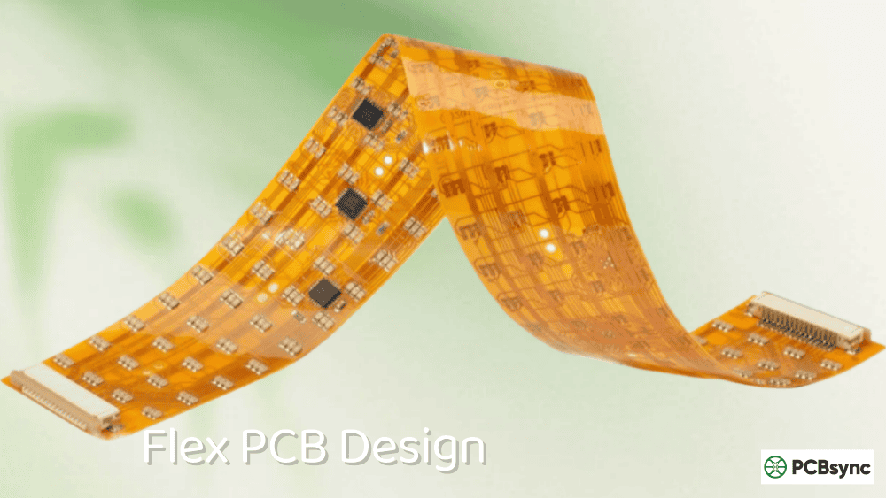
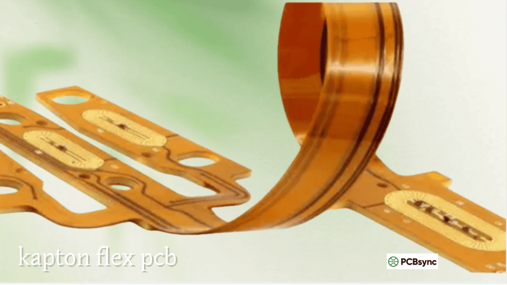
A 6 layer flex PCB is a flexible printed circuit board containing six conductive copper layers separated by flexible dielectric materials, typically polyimide. These layers are interconnected through plated through-holes, blind vias, and buried vias to create ultra-high-density interconnect structures while maintaining the ability to bend, fold, and conform to complex three-dimensional shapes.
The six-layer architecture represents a significant step up from four-layer flex. While 4 layer flex PCB handles most moderate-complexity applications adequately, 6 layer flex PCB addresses scenarios where routing density, signal integrity requirements, or power distribution complexity exceeds four-layer capabilities.
With six conductive layers, designers gain dedicated signal layers with complete ground and power plane references, multiple shielding options for sensitive circuits, and the routing capacity to handle high pin-count components like fine-pitch BGAs in a flexible format.
When to Choose 6 Layer Flex PCB Over Simpler Alternatives
The decision to use 6 layer flex PCB shouldn’t be made lightly—the cost and complexity increase substantially compared to four-layer designs. Here’s when it makes sense:
Routing Density Exceeds 4-Layer Capacity
When your design includes fine-pitch BGAs, high-density connectors, or complex mixed-signal circuits that simply won’t route on four layers, 6 layer flex PCB provides the additional channels needed. The two extra signal layers can double available routing capacity in constrained areas.
High-Speed Signal Integrity is Critical
Six layers allow optimal signal-ground-signal-power-ground-signal stack-ups where every signal layer has an immediately adjacent reference plane. This configuration minimizes crosstalk, maintains controlled impedance, and provides superior EMI performance compared to compromised four-layer arrangements.
Multiple Isolated Power Domains Required
Designs requiring separate analog and digital power distribution, multiple voltage rails, or isolated power sections benefit from the additional plane layers available in 6 layer flex PCB. Clean power separation becomes practical without sacrificing signal routing capacity.
Complex Mixed-Signal Designs
When analog and digital circuits must coexist on the same flexible substrate with complete isolation, six layers allow dedicated routing and reference planes for each domain.
High Channel Count Applications
Medical imaging, telecommunications, and data acquisition systems with dozens or hundreds of signal channels often require 6 layer flex PCB to achieve the necessary routing density while maintaining signal quality.
6 Layer Flex PCB Stack-Up Configurations
Stack-up design is critical for 6 layer flex PCB performance. The arrangement of signal, ground, and power layers directly impacts signal integrity, EMI performance, and manufacturing success.
This configuration provides optimal performance for most 6 layer flex PCB applications:
Layer
Function
Material
Typical Thickness
Reference Plane
Coverlay
Protection
PI + adhesive
25-50 μm
—
L1
High-speed signals
RA copper
12-18 μm (⅓-½ oz)
L2 (Ground)
Dielectric
Insulation
Polyimide
25-50 μm
—
L2
Ground plane
RA copper
12-18 μm
—
Core
Structural
Polyimide
50-75 μm
—
L3
Internal signals
RA copper
12-18 μm
L2 (Ground)
Dielectric
Insulation
Polyimide
25-50 μm
—
L4
Power plane
RA copper
12-18 μm
—
Core
Structural
Polyimide
50-75 μm
—
L5
Ground plane
RA copper
12-18 μm
—
Dielectric
Insulation
Polyimide
25-50 μm
—
L6
High-speed signals
RA copper
12-18 μm (⅓-½ oz)
L5 (Ground)
Coverlay
Protection
PI + adhesive
25-50 μm
—
Total thickness for a typical 6 layer flex PCB ranges from 0.3mm to 0.8mm depending on materials and copper weights.
Why Stack-Up Configuration Matters
Signal layers adjacent to reference planes: High-speed signals on L1 and L6 reference the immediately adjacent ground planes (L2 and L5), providing low-impedance return paths and excellent shielding. Internal signals on L3 also reference L2.
Power-ground plane pairing: L4 (power) sandwiched between L3 signals and L5 (ground) creates an effective capacitor for power delivery decoupling. This tight coupling improves power integrity at high frequencies.
Symmetrical construction: The balanced arrangement minimizes warping during manufacturing and provides consistent mechanical properties across the flex circuit.
Designing 6 layer flex PCB requires attention to flex-specific constraints that become more critical as layer count increases.
Trace Routing Best Practices
Parameter
Recommended Value
Notes
Minimum trace width
50-75 μm (2-3 mils)
HDI processes enable finer
Minimum spacing
50-75 μm (2-3 mils)
Match trace width
High-speed trace direction
Perpendicular to bend
Critical in flex zones
Via-to-bend distance
>2.0mm (80 mils)
Larger than 4-layer requirements
Trace stagger between layers
Offset 50%
Reduces stress concentration
Copper balance
Within 10% per side
Prevents warping
Critical Design Rules for 6 Layer Flex PCB
Route high-speed signals on outer layers: L1 and L6 have immediate ground plane references. Place critical high-frequency or sensitive signals here for best performance.
Use inner layers for less critical routing: L3 signals work well for slower digital, power distribution traces, and non-critical interconnects.
Avoid routing in flex zones: Where possible, keep traces out of dynamic bend areas entirely. When unavoidable, route perpendicular to the bend line with generous trace widths.
Minimize via count in flex regions: Each via creates a stress concentration point. Use blind vias to connect only necessary layers rather than through-holes penetrating all six layers.
Stagger traces vertically: Don’t stack traces directly above each other through the layer structure—offset them to distribute mechanical stress during flexing.
Bend Radius Requirements for 6 Layer Flex PCB
The increased thickness of 6 layer flex PCB requires larger bend radii than simpler constructions:
Application Type
Minimum Bend Radius
Example (0.5mm thickness)
Static (flex-to-install)
10-12× total thickness
5.0-6.0mm
Dynamic (repeated flexing)
20-30× total thickness
10.0-15.0mm
High-cycle dynamic
30-50× total thickness
15.0-25.0mm
These requirements are significantly more restrictive than four-layer flex. For applications requiring tight bend radii with high layer counts, consider rigid-flex construction where the flexible section uses fewer layers.
Via Strategies for 6 Layer Flex PCB
Via Type
Connects
Advantages
Considerations
Through-hole
All 6 layers
Simple, low cost
Maximum stress, avoid in flex zones
Blind via (L1-L2)
Outer to adjacent
Preserves flexibility
Requires sequential lamination
Blind via (L5-L6)
Outer to adjacent
Preserves flexibility
Requires sequential lamination
Buried via (L2-L5)
Inner layers only
Hidden from flex stress
Most complex, highest cost
Stacked microvia
Sequential layers
Maximum density
Multiple drill cycles
For best flex performance, minimize through-holes in bend zones and use blind or buried vias where layer-to-layer connections are required near flexible regions.
Manufacturing Considerations for 6 Layer Flex PCB
Manufacturing 6 layer flex PCB requires advanced capabilities and strict process controls. Understanding these requirements helps set realistic expectations for cost, lead time, and design constraints.
Manufacturing Process Overview
Sequential lamination: Unlike four-layer flex which can use single lamination, 6 layer flex PCB typically requires multiple lamination cycles. Inner layers (L2-L5) are fabricated first, then outer layers are laminated in subsequent cycles.
Precision registration: Six layers demand tighter registration accuracy than four-layer designs. Misalignment between layers can cause via-to-pad failures on inner layers that are impossible to inspect visually.
Controlled impedance verification: With signals on multiple layers referencing different planes, impedance control becomes more complex. Cross-section analysis and TDR testing verify actual impedance matches design targets.
Enhanced electrical testing: Hidden inner layers require comprehensive electrical testing. Flying probe or dedicated fixtures verify all connections since visual inspection can’t access inner layers.
Manufacturing Challenges Specific to 6 Layer Flex PCB
The combination of high routing density, excellent signal integrity, and mechanical flexibility makes 6 layer flex PCB essential for demanding applications across multiple industries.
Medical Device Applications
Application
Why 6 Layer Flex PCB
Key Requirements
Implantable neurostimulators
High channel count, extreme miniaturization
Ultra-thin, biocompatible, >10 year reliability
Endoscopic imaging systems
High-speed video, tight bend radii
Controlled impedance, dynamic flexing
Ultrasound transducers
Dense signal routing, EMI shielding
Fine pitch, high frequency performance
Cochlear implants
Maximum functionality in minimum volume
Multi-layer stiffener integration
Portable diagnostic equipment
Complex mixed-signal processing
Signal integrity, power management
Aerospace and Defense Applications
Application
Why 6 Layer Flex PCB
Key Requirements
Satellite communications
High-frequency routing, weight savings
Radiation tolerance, thermal cycling
Avionics displays
High-density interconnects
Controlled impedance, vibration resistance
Missile guidance systems
Extreme reliability, compact packaging
MIL-spec compliance, environmental resistance
UAV sensor integration
Multiple sensor channels, weight critical
Dynamic stress resistance
Night vision systems
Sensitive analog circuits, lightweight
Low noise, thermal management
Consumer Electronics Applications
Application
Why 6 Layer Flex PCB
Key Requirements
Foldable smartphones
Display connections, repeated folding
Ultra-high flex cycles, thin profile
VR/AR headsets
High-bandwidth display, compact form
High-speed digital, lightweight
Professional cameras
High-speed image sensor interfaces
Controlled impedance, vibration resistance
Premium audio equipment
Low-noise analog routing
EMI shielding, signal isolation
Gaming peripherals
High button/sensor density
Reliable dynamic flexing
Automotive Applications
Application
Why 6 Layer Flex PCB
Key Requirements
ADAS camera systems
High-speed video processing
Controlled impedance, thermal stability
EV battery management
Multi-cell monitoring, power distribution
High reliability, thermal cycling
Infotainment systems
Complex routing, space constraints
EMI compliance, vibration resistance
Autonomous driving sensors
LiDAR/radar signal processing
High-frequency performance
LED matrix headlights
High LED count, curved mounting
Thermal management, flexibility
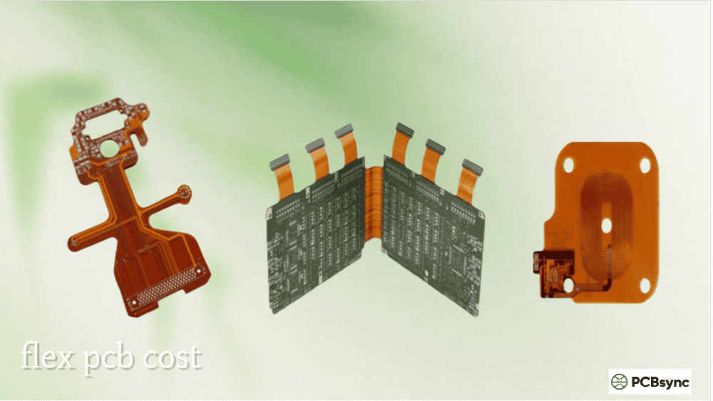
Cost Considerations for 6 Layer Flex PCB
Six-layer flex circuits represent a significant cost investment. Understanding cost drivers helps optimize designs and set appropriate budgets.
Cost Comparison by Layer Count
Specification
4 Layer Flex
6 Layer Flex PCB
8 Layer Flex
Relative cost
1× (baseline)
2-3×
4-6×
Prototype cost (typical)
$300-800
$800-2,000
$2,000-5,000+
Production cost/dm²
$100-250
$250-600
$600-1,500+
Lead time (prototype)
10-15 days
15-25 days
25-40 days
Lead time (production)
3-4 weeks
4-6 weeks
6-10 weeks
Cost Optimization Strategies for 6 Layer Flex PCB
Evaluate whether 6 layers are truly necessary: Before committing to 6 layer flex PCB, exhaust optimization possibilities on four layers. Sometimes creative routing, component repositioning, or design partitioning can achieve goals with simpler construction.
Minimize blind and buried vias: These require sequential drilling and add significant cost. Use through-holes where possible, reserving advanced via structures for areas where they’re essential.
Use standard materials: Exotic low-loss dielectrics or unusual copper weights increase cost. Standard polyimide and common thicknesses provide best value unless performance requirements mandate alternatives.
Optimize panel utilization: Work with your fabricator to maximize circuits per panel. Efficient panelization can reduce per-unit costs by 15-25%.
Consider rigid-flex alternatives: If only portions of your circuit require flexibility, rigid-flex construction may cost less than full 6 layer flex PCB by using rigid (cheaper) sections where appropriate.
Frequently Asked Questions About 6 Layer Flex PCB
What is the typical thickness of a 6 layer flex PCB?
Standard 6 layer flex PCB thickness ranges from 0.3mm to 0.8mm. The specific value depends on copper weight (typically ⅓ oz to ½ oz per layer for flexibility), dielectric thickness between layers (25-75 μm polyimide), and construction type. Ultra-thin builds using ⅓ oz copper and 25 μm dielectrics can achieve 0.3mm total thickness, while designs requiring heavier copper or thicker dielectrics for impedance control may approach 0.8mm. The increased thickness compared to 4-layer flex (0.2-0.6mm) directly impacts minimum bend radius requirements.
How does 6 layer flex PCB flexibility compare to 4-layer?
6 layer flex PCB is less flexible than 4-layer due to increased thickness. Minimum bend radii are approximately 50-100% larger for equivalent reliability. A 4-layer design might achieve 6mm static bend radius, while comparable 6-layer construction requires 10mm or more. For dynamic flexing applications, this difference becomes more pronounced. If your application requires tight bend radii with high layer count, consider rigid-flex construction where the flex sections use fewer layers, or evaluate whether the design can be partitioned differently.
When should I choose 6 layer flex PCB vs rigid-flex?
Choose pure 6 layer flex PCB when the entire circuit needs to be flexible or when you need a flexible interconnect without discrete rigid sections. Rigid-flex becomes preferable when significant component mounting requires rigid support, when different sections need different layer counts, or when the flex section can use fewer layers than the rigid sections. Rigid-flex typically costs more in simple configurations but can be more economical when it allows flex sections to use 2-4 layers while rigid sections carry the high layer count.
What surface finishes are recommended for 6 layer flex PCB?
ENIG (Electroless Nickel Immersion Gold) is the standard choice for 6 layer flex PCB, providing excellent solderability, flat surfaces for fine-pitch components, and good shelf life. Immersion silver offers good performance at lower cost for less demanding applications. For flex circuits requiring repeated connector insertion, hard gold plating on contact areas provides wear resistance. Avoid HASL on thin flex—the thermal stress can cause warping, and the uneven surface is incompatible with fine-pitch components common in high-density 6-layer designs.
What is the typical prototype lead time for 6 layer flex PCB?
Prototype lead times for 6 layer flex PCB typically run 15-25 business days, compared to 10-15 days for 4-layer flex. The extended time reflects sequential lamination requirements, additional imaging/etching cycles, and more rigorous testing. Premium expedited services may reduce this to 10-15 days at significant cost premiums (often 75-150% of base price). Production quantities typically require 4-6 weeks. Complex designs with blind/buried vias, unusual materials, or tight tolerances can extend these timelines further.
Useful Resources for 6 Layer Flex PCB Design
Industry Standards
IPC-6013: Qualification and Performance Specification for Flexible/Rigid-Flexible Printed Boards
IPC-2223: Sectional Design Standard for Flexible Printed Boards
IPC-A-610: Acceptability of Electronic Assemblies
IPC-4204: Specification for Adhesive Coated Dielectric Films
Design Software with Advanced Flex Support
Altium Designer: www.altium.com – Layer Stack Manager, flex regions
Making the Decision: Is 6 Layer Flex PCB Right for Your Design?
6 layer flex PCB is the right choice when:
Four-layer routing capacity is genuinely exhausted
Signal integrity requirements demand dedicated reference planes for all signal layers
Multiple isolated power domains are essential
High channel count applications exceed 4-layer routing density
The cost and lead time premium is justified by application requirements
Stay with 4-layer flex when:
Routing can be accomplished with creative optimization
Maximum flexibility is priority (thinner = more flexible)
Budget constraints are significant
Lead time is critical
Bend radius requirements are tight
Consider 8+ layer flex when:
Six layers can’t accommodate the routing
Extreme density with complete shielding is required
Cost is secondary to performance
That neural interface project I started this article with? After thousands of hours in the field, those 6 layer flex PCB circuits are still functioning perfectly. The extra two layers gave us the routing density for 128 channels, the shielding to maintain signal quality, and just enough flexibility to achieve the required form factor. Six layers were exactly what that application needed—not more, not less.
When your design genuinely requires the capabilities that 6 layer flex PCB provides, the investment pays off in functionality that simpler constructions simply cannot deliver. The key is making that determination honestly, based on actual requirements rather than design convenience.
Inquire: Call 0086-755-23203480, or reach out via the form below/your sales contact to discuss our design, manufacturing, and assembly capabilities.
Quote: Email your PCB files to Sales@pcbsync.com (Preferred for large files) or submit online. We will contact you promptly. Please ensure your email is correct.
Notes: For PCB fabrication, we require PCB design file in Gerber RS-274X format (most preferred), *.PCB/DDB (Protel, inform your program version) format or *.BRD (Eagle) format. For PCB assembly, we require PCB design file in above mentioned format, drilling file and BOM. Click to download BOM template To avoid file missing, please include all files into one folder and compress it into .zip or .rar format.


