Inquire: Call 0086-755-23203480, or reach out via the form below/your sales contact to discuss our design, manufacturing, and assembly capabilities.
Quote: Email your PCB files to Sales@pcbsync.com (Preferred for large files) or submit online. We will contact you promptly. Please ensure your email is correct.
Notes: For PCB fabrication, we require PCB design file in Gerber RS-274X format (most preferred), *.PCB/DDB (Protel, inform your program version) format or *.BRD (Eagle) format. For PCB assembly, we require PCB design file in above mentioned format, drilling file and BOM. Click to download BOM template To avoid file missing, please include all files into one folder and compress it into .zip or .rar format.
The first time I designed a 4 layer flex PCB, I was working on a medical endoscope camera module. The client needed high-speed differential pairs, a solid ground plane for EMI control, and the whole thing had to navigate a 180-degree bend through a 12mm diameter tube. Two-layer flex couldn’t deliver the routing density or signal integrity we needed. That project taught me what four-layer flex circuits really bring to the table—and when the added complexity is justified.
If you’re evaluating whether 4 layer flex PCB fits your application, or you’re already committed and need stack-up guidance, this article covers the essential configurations, manufacturing considerations, and real-world applications where multilayer flex delivers results that simpler constructions can’t match.
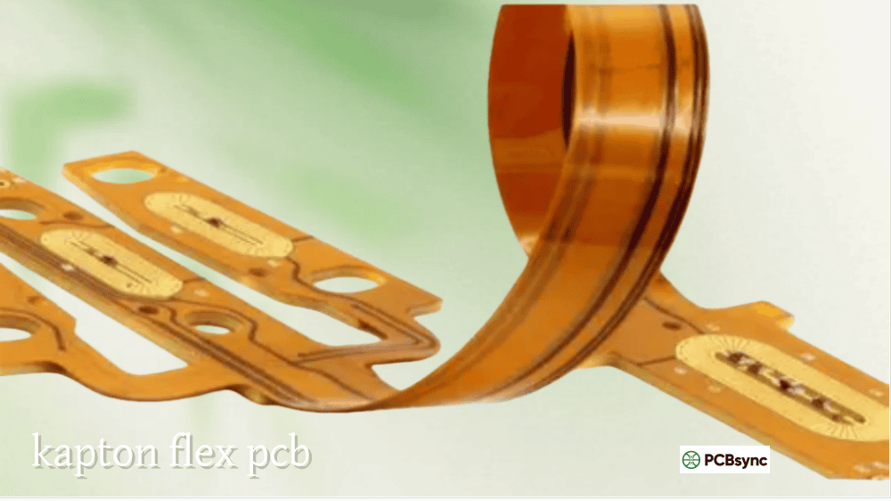
A 4 layer flex PCB is a flexible printed circuit board containing four conductive copper layers separated by flexible dielectric materials, typically polyimide. These four layers are interconnected through plated through-holes (PTHs), blind vias, or buried vias, creating a high-density interconnect structure that bends, folds, and conforms to three-dimensional shapes.
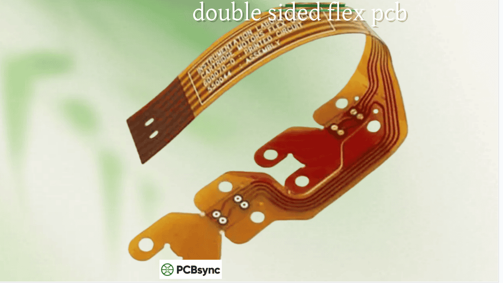
Unlike simpler single or double-sided flex circuits, 4 layer flex PCB provides dedicated layers for signals, ground planes, and power distribution. This architecture enables controlled impedance routing, integrated EMI shielding, and complex circuit topologies in a package that still flexes during installation or operation.
The four conductive layers dramatically increase routing density compared to two-layer designs. Where a double-sided flex might struggle with signal crossovers and ground return paths, 4 layer flex PCB handles these challenges elegantly through proper layer assignment and via structures.
4 Layer Flex PCB Stack-Up Configurations
Stack-up design is where 4 layer flex PCB projects succeed or fail. The arrangement of signal, ground, and power layers directly impacts signal integrity, EMI performance, impedance control, and mechanical flexibility.
Common 4 Layer Flex PCB Stack-Up Options
Configuration
Layer 1
Layer 2
Layer 3
Layer 4
Best Application
Signal-Ground-Power-Signal
Signal
Ground
Power
Signal
General purpose, good EMI
Signal-Ground-Ground-Signal
Signal
Ground
Ground
Signal
High-speed digital, best EMI
Signal-Power-Ground-Signal
Signal
Power
Ground
Signal
Mixed signal designs
Signal-Signal-Ground-Ground
Signal
Signal
Ground
Ground
High routing density needs
Standard 4 Layer Flex PCB Stack-Up Structure
Layer Position
Material
Typical Thickness
Function
Top Coverlay
Polyimide + adhesive
25-50 μm
Protects outer traces
Layer 1 (Signal)
RA or ED copper
12-35 μm (⅓-1 oz)
Top signal routing
Adhesive
Acrylic/epoxy
12.5-25 μm
Bonds Layer 1 to core
Core Dielectric 1
Polyimide
25-50 μm
Insulates L1 from L2
Layer 2 (Ground)
RA or ED copper
12-35 μm
Ground reference plane
Core Dielectric 2
Polyimide
25-75 μm
Central flexible core
Layer 3 (Power)
RA or ED copper
12-35 μm
Power distribution
Core Dielectric 3
Polyimide
25-50 μm
Insulates L3 from L4
Adhesive
Acrylic/epoxy
12.5-25 μm
Bonds Layer 4 to core
Layer 4 (Signal)
RA or ED copper
12-35 μm (⅓-1 oz)
Bottom signal routing
Bottom Coverlay
Polyimide + adhesive
25-50 μm
Protects outer traces
Total thickness for a typical 4 layer flex PCB ranges from 0.2mm to 0.6mm, depending on copper weights, dielectric thicknesses, and whether adhesive-based or adhesiveless construction is used.
Choosing the Right Stack-Up for Your 4 Layer Flex PCB
Signal-Ground-Power-Signal is the most versatile configuration. It provides a ground reference plane adjacent to Layer 1 signals for controlled impedance, while Layer 4 signals reference the power plane. This arrangement works well for most applications requiring moderate high-speed performance.
Signal-Ground-Ground-Signal offers the best EMI performance and signal integrity. Both outer signal layers have an immediately adjacent ground plane, providing optimal return current paths and shielding. Use this when high-speed digital signals or RF circuits are critical.
Signal-Power-Ground-Signal distributes power and ground on opposite sides of the core, which can simplify power distribution in designs with heavy current requirements on both board surfaces.
Signal-Signal-Ground-Ground maximizes routing density by dedicating two layers to signals, but compromises signal integrity since Layer 2 signals don’t have an immediately adjacent reference plane.
Benefits of 4 Layer Flex PCB Technology
Moving from two-layer to 4 layer flex PCB isn’t just about adding routing channels. The four-layer architecture enables capabilities that fundamentally change what’s possible in a flexible circuit.
Maximum Routing Density
Four conductive layers provide dramatically more routing real estate. Complex, compact layouts with hundreds of connections become manageable when you can distribute traces across four layers instead of two. Fine-pitch BGA breakouts, dense connector interfaces, and intricate analog/digital mixed circuits all benefit from the additional routing layers.
Integrated EMI/RFI Shielding
Entire copper layers can function as electromagnetic shields. A continuous ground plane in Layer 2 shields Layer 1 signals from internal noise sources, while also preventing emissions from escaping the circuit. This integrated shielding often eliminates the need for external EMI shields or additional shielding components.
Controlled Impedance Performance
Proper 4 layer flex PCB stack-ups enable precise impedance control for high-speed signals. The consistent dielectric thickness between signal and reference layers allows calculation and achievement of target impedances (typically 50Ω single-ended or 100Ω differential). High-frequency and high-speed digital applications depend on this capability.
Enhanced Signal Integrity
Dedicated ground and power planes provide low-inductance return current paths, reducing ground bounce, crosstalk, and power supply noise. Differential pair routing with consistent reference planes maintains signal quality across the entire circuit length.
Space and Weight Reduction
Four-layer construction packs complex circuits into minimal volume. The elimination of cables, connectors, and separate PCB assemblies reduces overall system weight—critical in aerospace, portable medical devices, and wearable electronics where every gram matters.
Component Density Improvement
With escape routing distributed across four layers, component placement becomes more flexible. Dense component clusters that would require impossible routing on two-layer flex become practical when additional layers provide breakout paths.
Embedded Passive Integration
Advanced 4 layer flex PCB designs can incorporate embedded resistors, capacitors, and inductors within the layer structure, further reducing component count and assembly complexity.
Manufacturing 4 layer flex PCB demands precision beyond what simpler flex circuits require. The process involves multiple lamination cycles, careful layer registration, and specialized handling throughout.
Key Manufacturing Steps
Step 1: Inner Layer Fabrication The process begins by fabricating the inner copper layers (Layers 2 and 3) on flexible copper-clad laminates. These cores are drilled, plated, imaged, and etched to create the inner circuit patterns.
Step 2: Layup and Lamination Inner layers are stacked with adhesive sheets and outer copper foils in precise alignment. The assembly undergoes lamination under controlled heat and pressure, bonding all layers into a unified structure.
Step 3: Through-Hole Drilling Mechanical or laser drilling creates via holes connecting multiple layers. Registration accuracy is critical—misaligned holes can miss capture pads on inner layers.
Step 4: Hole Plating Drilled holes are plated with copper to establish electrical connections between layers. Uniform plating thickness on via walls ensures reliable interconnections that survive flexing.
Step 5: Outer Layer Imaging Photoresist is applied to outer copper surfaces, exposed with the circuit pattern, and developed to define outer layer traces.
Step 6: Outer Layer Etching Chemical etching removes unwanted copper from outer layers, leaving the designed circuit patterns.
Step 7: Coverlay Application Polyimide coverlay films are aligned and laminated over outer layers, protecting traces while maintaining flexibility.
Step 8: Surface Finish Exposed pads receive surface finish (ENIG, immersion tin, OSP) for solderability and oxidation protection.
Step 9: Electrical Testing Comprehensive continuity and isolation testing verifies all connections. Four-layer circuits require thorough testing given the hidden inner layers.
Step 10: Profiling and Final Inspection Circuits are cut from panels, inspected for defects, and prepared for shipment.
Manufacturing Challenges Specific to 4 Layer Flex PCB
Challenge
Impact
Mitigation Approach
Layer Registration
Misalignment causes via-to-pad failures
Optical alignment systems, precision tooling
Fine Line Resolution
4 layers demand finer traces for density
Advanced imaging, controlled etching
Microvia Reliability
Blind/buried vias must survive flexing
Proper aspect ratios, adequate plating
Impedance Control
Tight tolerances across flexible layers
Material selection, process control
Delamination Risk
Multiple adhesive interfaces can fail
Proper adhesive selection, lamination control
Flex Cycle Endurance
More layers increase fatigue stress
Material selection, design for flex zones
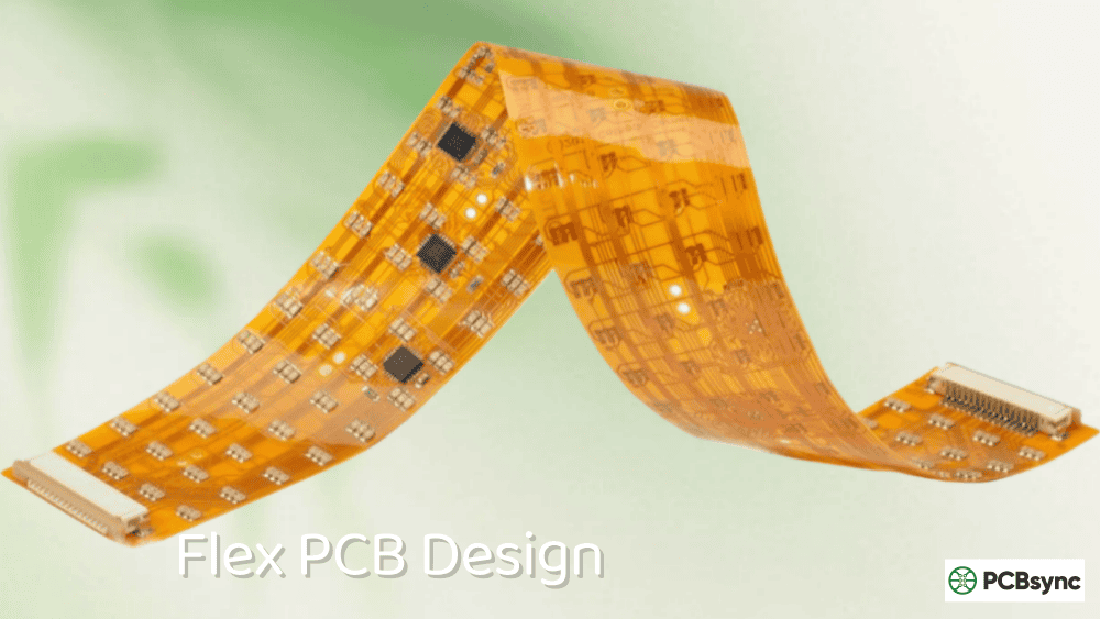
4 Layer Flex PCB Design Guidelines
Successful 4 layer flex PCB designs require attention to flex-specific rules beyond standard rigid board practices.
Trace Routing Best Practices
Parameter
Recommended Value
Notes
Minimum Trace Width
75-100 μm (3-4 mils)
Narrower possible with HDI processes
Minimum Spacing
75-100 μm (3-4 mils)
Match trace width for manufacturability
Trace Direction in Flex Zones
Perpendicular to bend
Reduces stress on copper traces
Via-to-Bend Distance
>1.5mm (60 mils) minimum
Prevents via cracking during flexing
Stagger Traces Between Layers
Offset by half trace pitch
Reduces stress concentration
Copper Distribution
Balance copper on all layers
Prevents warping and stress
Bend Radius Requirements for 4 Layer Flex PCB
The minimum bend radius for 4 layer flex PCB is larger than two-layer designs due to increased thickness:
Application Type
Minimum Bend Radius
Notes
Static (flex-to-install)
6-10× total thickness
One-time bend during assembly
Dynamic (repeated flexing)
15-25× total thickness
Continuous or repeated bending
High-cycle dynamic
25-40× total thickness
Millions of flex cycles required
For a 0.4mm thick 4 layer flex PCB:
Static applications: 2.4-4.0mm minimum bend radius
Dynamic applications: 6.0-10.0mm minimum bend radius
Via and Interconnect Considerations
Through-holes connect all four layers but limit flexibility in bend zones. Keep PTHs in static areas with stiffeners.
Blind vias connect outer layers to adjacent inner layers (L1-L2 or L3-L4), providing routing flexibility without penetrating the full stack.
Buried vias connect inner layers only (L2-L3), useful for internal routing that doesn’t require outer layer access.
Stacked vs. staggered vias: Staggered via placement distributes stress better in flex zones.
The combination of high routing density, controlled impedance, and mechanical flexibility makes 4 layer flex PCB essential across demanding industries.
Medical Device Applications
Medical devices frequently require 4 layer flex PCB for miniaturization and reliability in critical applications:
Application
Why 4 Layer Flex PCB
Key Requirements
Endoscopes
High-speed imaging, tight bend radii
Controlled impedance, biocompatibility
Ultrasound Transducers
Dense signal routing, EMI shielding
Fine pitch, high channel count
Implantable Devices
Maximum miniaturization
Ultra-thin, high reliability
Patient Monitors
Multi-sensor integration
Mixed analog/digital routing
Hearing Aids
Extreme space constraints
Minimum thickness, high density
Aerospace and Defense Applications
Weight reduction and reliability drive aerospace adoption of 4 layer flex PCB:
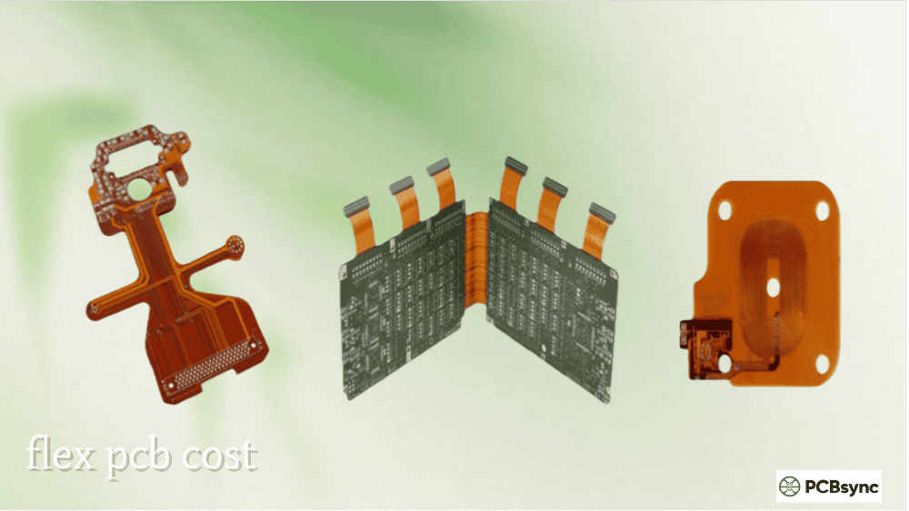
Four-layer flex circuits cost significantly more than simpler constructions. Understanding cost drivers helps optimize designs and budgets.
Cost Comparison by Layer Count
Specification
2 Layer Flex
4 Layer Flex PCB
6 Layer Flex
Relative Cost
1× (baseline)
2.5-4×
5-8×
Prototype Cost (typical)
$100-300
$300-800
$800-2000+
Production Cost/dm²
$40-80
$100-250
$250-500+
Lead Time (prototype)
5-10 days
10-15 days
15-25 days
Lead Time (production)
2-3 weeks
3-4 weeks
4-6 weeks
Strategies to Optimize 4 Layer Flex PCB Costs
Minimize layer count where possible: If your design can work with strategic two-layer flex plus stiffeners, the cost savings are substantial.
Reduce via complexity: Through-holes cost less than blind/buried vias. Use the simplest via structure that meets requirements.
Optimize panel utilization: Work with your fabricator to maximize boards per panel, reducing per-unit costs.
Standardize materials: Custom dielectric thicknesses or exotic materials increase cost. Use standard material combinations when performance allows.
Design for manufacturability: Generous tolerances, adequate spacing, and proper design rules reduce yields losses and rework.
Frequently Asked Questions About 4 Layer Flex PCB
What is the typical thickness of a 4 layer flex PCB?
Standard 4 layer flex PCB thickness ranges from 0.2mm to 0.6mm. The specific value depends on copper weight (typically ⅓ oz to 1 oz per layer), dielectric thickness (25-75 μm polyimide), and construction type (adhesive-based versus adhesiveless). Ultra-thin designs using 12.5 μm substrates and ⅓ oz copper can achieve thicknesses below 0.2mm, while designs with heavier copper or thicker dielectrics for impedance control may approach 0.6mm.
Can 4 layer flex PCB handle dynamic flexing applications?
Yes, but with important design constraints. For dynamic flexing, use rolled annealed (RA) copper, maintain generous bend radii (15-25× thickness minimum), route traces perpendicular to bend lines, avoid vias in flex zones, and consider adhesiveless construction for improved fatigue resistance. Well-designed 4 layer flex PCB can achieve 10 million+ flex cycles, though this is lower than single or double-layer flex due to increased thickness and layer count.
How does 4 layer flex PCB compare to rigid-flex for my application?
Pure 4 layer flex PCB is appropriate when the entire circuit requires flexibility or when you need a flexible interconnect without rigid mounting areas. Rigid-flex combines rigid sections (for component mounting and mechanical stability) with flexible interconnects, eliminating board-to-board connectors. Choose rigid-flex when significant components require rigid mounting surfaces, or when the design needs both stiff sections and flexible connections. Rigid-flex typically costs more than pure flex due to additional manufacturing complexity.
What surface finishes work best for 4 layer flex PCB?
ENIG (Electroless Nickel Immersion Gold) is the most common choice for 4 layer flex PCB, offering excellent solderability, flat surfaces for fine-pitch components, and good shelf life. Immersion silver provides good performance at lower cost but has shorter shelf life. OSP (Organic Solderability Preservative) works for immediate assembly applications. Hard gold is specified for edge connectors or contact areas subject to repeated mating cycles. Avoid HASL (Hot Air Solder Leveling) on thin flex circuits due to thermal stress concerns.
What is the typical lead time for 4 layer flex PCB prototypes?
Standard prototype lead times for 4 layer flex PCB run 10-15 business days, compared to 5-10 days for two-layer flex. Expedited services can reduce this to 5-7 days at premium pricing (typically 50-100% rush charges). Production quantities require 3-4 weeks for standard delivery. Factors extending lead time include exotic materials, tight tolerances, complex via structures (blind/buried), unusual surface finishes, and stiffener requirements.
Useful Resources for 4 Layer Flex PCB Design
Industry Standards
IPC-6013: Qualification and Performance Specification for Flexible/Rigid-Flexible Printed Boards
IPC-2223: Sectional Design Standard for Flexible Printed Boards
Making the Decision: When 4 Layer Flex PCB Makes Sense
4 layer flex PCB is the right choice when:
Routing complexity exceeds two-layer capabilities
Controlled impedance is required for high-speed signals
EMI shielding must be integrated into the circuit
Space constraints demand maximum routing density
The application requires both flexibility and complex circuitry
Consider simpler alternatives when:
Basic point-to-point connections suffice
Maximum flexibility is the priority (fewer layers flex easier)
Budget constraints are severe
Lead time is critical and expedited flex isn’t available
Evaluate rigid-flex instead when:
Significant components require rigid mounting areas
The design combines flexible interconnects with rigid functional sections
Board-to-board connectors would otherwise be required
That endoscope project I mentioned at the start? The 4 layer flex PCB we designed has been in production for eight years now, installed in thousands of units navigating through patients’ bodies daily. The four-layer architecture delivered the signal integrity the imaging system demanded while surviving the mechanical environment that would have destroyed lesser designs. That’s what properly designed multilayer flex can accomplish.
When your application truly needs the capabilities that 4 layer flex PCB provides—controlled impedance, integrated shielding, high-density routing in a flexible package—nothing else will do. The cost and complexity are real, but so are the results.
Inquire: Call 0086-755-23203480, or reach out via the form below/your sales contact to discuss our design, manufacturing, and assembly capabilities.
Quote: Email your PCB files to Sales@pcbsync.com (Preferred for large files) or submit online. We will contact you promptly. Please ensure your email is correct.
Notes: For PCB fabrication, we require PCB design file in Gerber RS-274X format (most preferred), *.PCB/DDB (Protel, inform your program version) format or *.BRD (Eagle) format. For PCB assembly, we require PCB design file in above mentioned format, drilling file and BOM. Click to download BOM template To avoid file missing, please include all files into one folder and compress it into .zip or .rar format.


