Overview of the XC3130A-3PC84C FPGA
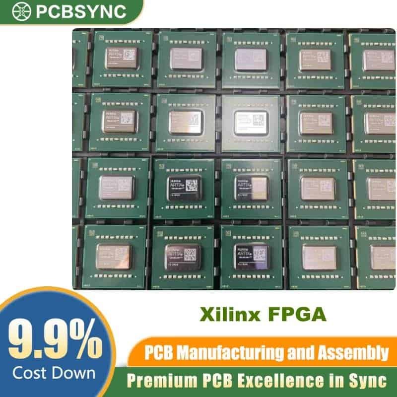
The XC3130A-3PC84C is a powerful Field Programmable Gate Array (FPGA) from the renowned XC3000A series, manufactured by AMD (formerly Xilinx). This programmable logic device delivers exceptional performance for embedded systems, industrial automation, and digital signal processing applications. With its 100 configurable logic blocks and 84-pin PLCC package, the XC3130A-3PC84C FPGA provides engineers with a flexible, reliable solution for complex digital designs.
As part of the proven Xilinx FPGA family, this device combines high-density logic capabilities with industry-standard packaging, making it an ideal choice for both prototype development and production-scale deployment.
Key Technical Specifications
Core Performance Parameters
| Specification |
Value |
| Part Number |
XC3130A-3PC84C |
| Family |
XC3000A/L Series |
| Configurable Logic Blocks (CLBs) |
100 (10×10 array) |
| Maximum User I/O |
80 pins |
| Gate Count Equivalent |
~3,000 gates |
| RAM Bits |
2,700 bits |
| Operating Frequency |
Up to 270 MHz |
| Propagation Delay |
2.7 ns |
| Speed Grade |
-3 (high performance) |
Package and Physical Characteristics
| Feature |
Description |
| Package Type |
84-LCC (J-Lead) / PLCC84 |
| Total Pins |
74 functional I/O pins |
| Technology |
CMOS |
| Operating Temperature Range |
0°C to +85°C (Commercial) |
| Supply Voltage |
5V nominal |
| Lead Compliance |
Contains Lead (legacy component) |
Architecture Features
| Component |
Specification |
| Tri-state Buses |
20 internal buses |
| Tri-state Buffers per Bus |
11 buffers |
| Global Clock Buffers |
2 |
| Crystal Oscillator Amplifier |
1 |
| Configuration Storage |
SRAM-based |
Product Features and Benefits
Advanced FPGA Architecture
The XC3130A-3PC84C features the Logic Cell Array (LCA) architecture that revolutionized programmable logic design. This architecture consists of three primary configurable elements:
- Configurable Logic Blocks (CLBs): 100 CLBs arranged in a 10×10 matrix provide the computational core
- Input/Output Blocks (IOBs): Peripheral IOBs enable flexible interfacing with external components
- Programmable Interconnect: Sophisticated routing resources connect CLBs and IOBs with minimal delay
High-Performance Digital Processing
With a maximum operating frequency of 270 MHz and propagation delay of just 2.7 ns, this FPGA excels in time-critical applications. The -3 speed grade designation indicates optimized performance characteristics for demanding digital signal processing tasks.
Flexible I/O Configuration
The 84-pin PLCC package provides up to 80 user-programmable I/O pins, offering exceptional flexibility for custom peripheral interfacing. Each IOB supports multiple I/O standards and can be independently configured for input, output, or bidirectional operation.
Internal Memory Resources
The device includes 2,700 bits of distributed RAM within the CLB structure, enabling efficient implementation of small memory buffers, lookup tables, and shift registers without consuming external resources.
Application Areas
Industrial Control Systems
The XC3130A-3PC84C excels in industrial automation applications, including:
- Programmable Logic Controllers (PLCs)
- Motor control systems
- Sensor interface circuits
- Industrial protocol converters
Digital Signal Processing
Ideal for DSP applications requiring:
- Digital filtering
- Data acquisition systems
- Real-time signal analysis
- Communication protocol implementation
Embedded Systems Development
Perfect for embedded applications such as:
- Custom peripheral controllers
- State machine implementation
- Hardware acceleration modules
- Prototype development and validation
Legacy System Maintenance
As a mature, proven technology, this FPGA is essential for:
- Replacement parts for existing systems
- Long-term product support
- Maintaining critical infrastructure
- Reverse engineering projects
Design Development Support
Development Tools Compatibility
The XC3130A-3PC84C is supported by comprehensive development tools:
- XACT Development System: Schematic capture and auto place-and-route
- ISE Design Suite: Legacy tool support for XC3000 series
- Logic Simulation: VHDL and Verilog simulation capabilities
- In-Circuit Emulation: Hardware verification options
CAD Integration
Multiple CAD formats are available for seamless PCB integration, including:
- Altium Designer libraries
- Eagle CAD footprints
- OrCAD symbols
- KiCAD components
- PADS layouts
Package and Ordering Information
Package Type Details
The 84-LCC (J-Lead) package features:
- Leadless Chip Carrier design with J-bent leads
- Square package footprint for efficient PCB layout
- Compatible with standard PLCC sockets for prototyping
- Surface-mount and through-hole socket options
- Industry-standard dimensions for easy replacement
Part Number Breakdown
Understanding the XC3130A-3PC84C nomenclature:
- XC = Xilinx FPGA product line
- 3130A = XC3000A family, 3,000-gate equivalent device
- -3 = Speed grade (-3 indicates high performance)
- PC84 = Plastic PLCC package with 84 pins
- C = Commercial temperature range (0°C to 85°C)
Why Choose the XC3130A-3PC84C?
Proven Reliability
With decades of deployment in mission-critical applications, the XC3000A series has established an unparalleled reputation for reliability. This FPGA has been tested in harsh industrial environments and continues to deliver consistent performance.
Cost-Effective Solution
For established designs and legacy system support, the XC3130A-3PC84C offers:
- Predictable supply chain for long-term projects
- Competitive pricing for volume orders
- Reduced development costs with proven architecture
- Extensive documentation and community support
Industry Standard Compatibility
The device complies with industry standards for:
- Programmable logic device specifications
- J-STD-020 moisture sensitivity levels
- IPC standards for PCB mounting
- ESD protection requirements
Technical Support and Resources
Documentation Availability
Comprehensive technical resources include:
- Complete datasheet with electrical specifications
- Application notes for common implementations
- Reference designs and example code
- Migration guides from other FPGA families
Design Assistance
Engineers benefit from:
- Active technical forums and community support
- Legacy design consultation services
- CAD library downloads for major design tools
- Online calculators for power and timing analysis
Comparison with Related Products
XC3000A Series Alternatives
| Part Number |
CLBs |
Max I/O |
Speed Grade |
Package Options |
| XC3020A |
64 |
64 |
-3, -4 |
PC44, PC68, PQ100 |
| XC3130A |
100 |
80 |
-3, -4 |
PC84, PQ100, VQ100 |
| XC3142A |
144 |
96 |
-3, -4, -5 |
PC84, PQ100 |
| XC3164A |
224 |
120 |
-3, -4 |
PC84, PQ160 |
Speed Grade Performance
| Speed Grade |
Max Frequency |
Propagation Delay |
Application Focus |
| -09 |
~200 MHz |
3.5 ns |
Low-power, cost-sensitive |
| -2 |
~230 MHz |
3.0 ns |
Standard performance |
| -3 |
~270 MHz |
2.7 ns |
High-performance |
| -4 |
~300 MHz |
2.4 ns |
Maximum speed |
Procurement Considerations
Availability and Sourcing
The XC3130A-3PC84C is available through:
- Authorized distributors like Digi-Key Electronics
- Electronic component brokers
- Surplus and obsolete parts specialists
- Direct manufacturer channels for volume orders
Stock Status and Lead Times
As a mature product:
- Generally available from multiple sources
- Lead times vary by distributor
- Consider stocking for critical applications
- Plan for potential obsolescence management
Quality Assurance
When purchasing, verify:
- Authentic manufacturer markings
- Date codes and lot traceability
- Proper ESD-safe packaging
- Authorized distributor certification
- Moisture sensitivity level (MSL) compliance
Environmental and Compliance Information
Material Composition
The XC3130A-3PC84C contains lead in its construction, which is important for:
- RoHS exemptions in legacy equipment
- Proper disposal and recycling procedures
- Compliance documentation requirements
- Import/export considerations
Operating Environment
Designed for commercial temperature applications:
- Operating range: 0°C to +85°C
- Storage range: -55°C to +125°C
- Humidity tolerance: 0% to 95% non-condensing
- Suitable for most industrial environments
Conclusion
The XC3130A-3PC84C FPGA represents a mature, reliable solution for digital design applications requiring proven performance and long-term availability. As part of the legendary Xilinx FPGA family, this device continues to serve critical roles in industrial control, embedded systems, and legacy equipment maintenance.
With its 100 configurable logic blocks, 80 I/O pins, and 270 MHz performance capability, the XC3130A-3PC84C delivers the perfect balance of functionality, reliability, and cost-effectiveness for engineers worldwide. Whether you’re maintaining existing systems or developing new applications with proven technology, this FPGA offers the features and support needed for successful project completion.
For detailed technical specifications, pricing information, and availability, consult authorized distributors and the comprehensive datasheet documentation available through official channels.
![]()


