Inquire: Call 0086-755-23203480, or reach out via the form below/your sales contact to discuss our design, manufacturing, and assembly capabilities.
Quote: Email your PCB files to Sales@pcbsync.com (Preferred for large files) or submit online. We will contact you promptly. Please ensure your email is correct.
Notes: For PCB fabrication, we require PCB design file in Gerber RS-274X format (most preferred), *.PCB/DDB (Protel, inform your program version) format or *.BRD (Eagle) format. For PCB assembly, we require PCB design file in above mentioned format, drilling file and BOM. Click to download BOM template To avoid file missing, please include all files into one folder and compress it into .zip or .rar format.
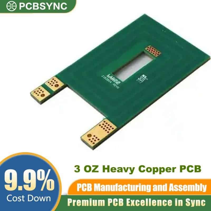
After spending 15 years designing power electronics, I’ve learned that choosing the right copper weight can make or break a project. When standard 1 oz or 2 oz copper just won’t cut it for high-current applications, engineers turn to heavy copper solutions like 9 oz PCB. This guide covers everything you need to know about 9 oz copper PCB design, from thickness specifications to real-world applications.
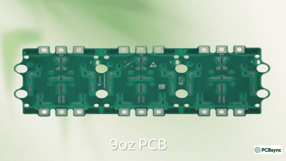
What is a 9 oz PCB?
A 9 oz PCB refers to a printed circuit board with copper layers weighing 9 ounces per square foot. In the PCB industry, copper thickness is measured by weight rather than linear dimensions. When 9 ounces of copper is flattened to cover one square foot of surface area, it produces a layer approximately 12.33 mils (0.313mm) thick.
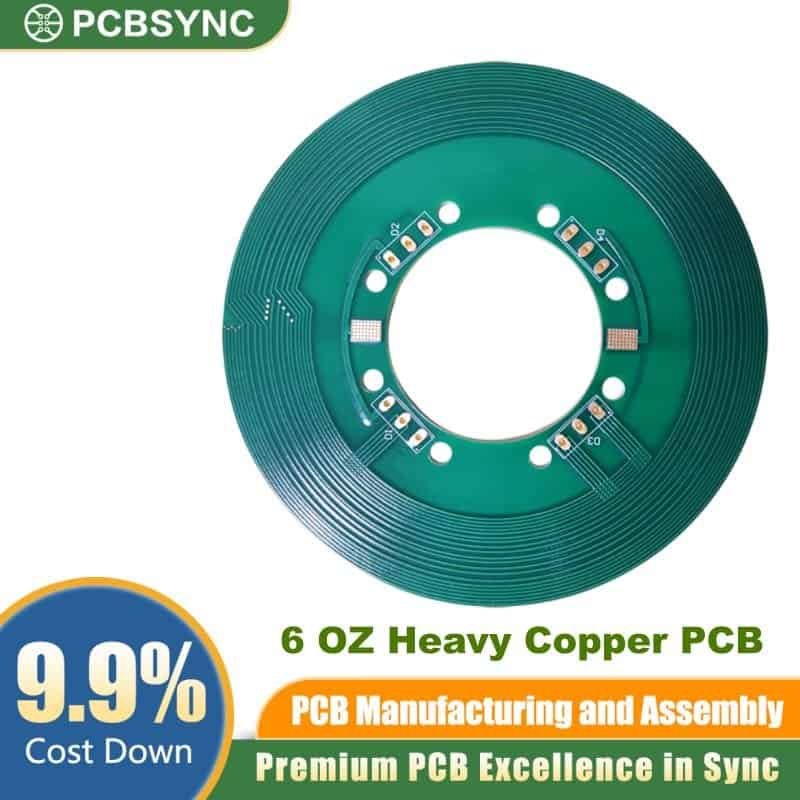
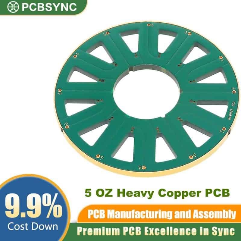
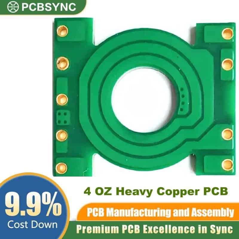
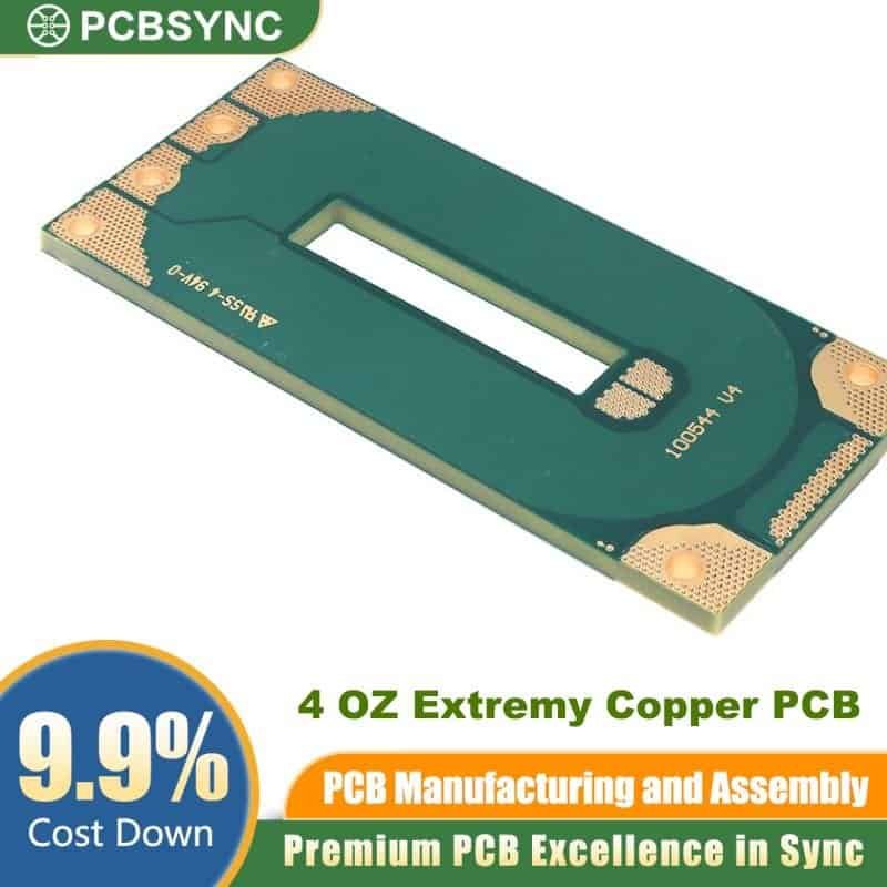
This puts 9 oz PCB firmly in the “heavy copper” category. While standard PCBs use 1 oz to 2 oz copper (the industry default), anything above 3 oz is considered heavy copper. At 9 oz, you’re working with copper that’s roughly nine times thicker than standard boards, which opens up possibilities for high-power applications that would destroy conventional PCBs.
Understanding the relationship between copper weight and actual thickness is crucial for design decisions. Here’s a comprehensive conversion table:
Copper Weight
Thickness (mils)
Thickness (mm)
Thickness (μm)
Category
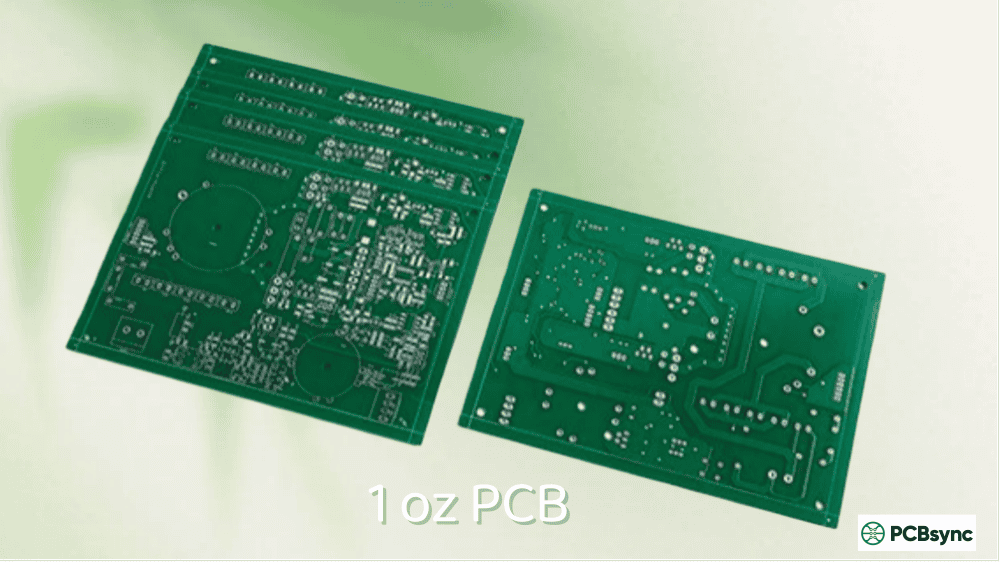
1 oz
1.37
0.035
35
Standard
2 oz
2.74
0.070
70
Standard
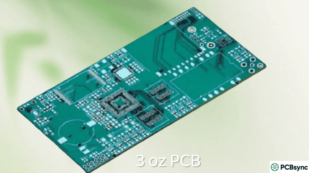
3 oz
4.11
0.105
105
Heavy
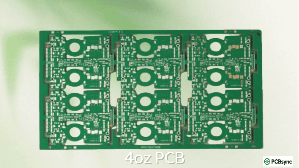
4 oz
5.48
0.140
140
Heavy
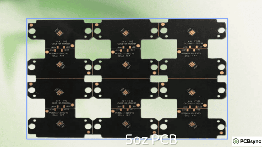
6 oz
8.22
0.209
209
Heavy
9 oz
12.33
0.313
313
Heavy
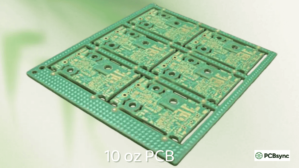
10 oz
13.70
0.348
348
Heavy
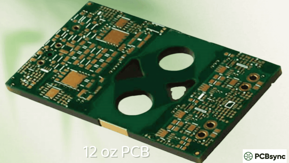
12 oz
16.44
0.418
418
Extreme
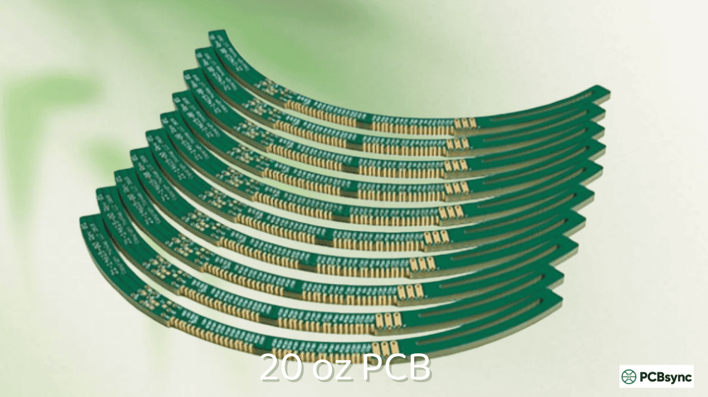
20 oz
27.40
0.696
696
Extreme
Note: The highlighted row shows 9 oz PCB specifications. Values are based on the industry standard where 1 oz of copper spread over 1 square foot equals 1.37 mils thickness.
Why Choose 9 oz PCB for Your Design?
Selecting 9 oz copper isn’t arbitrary—it solves specific engineering challenges that lighter copper weights simply cannot address. Here’s when 9 oz PCB becomes the right choice:
High Current Carrying Capacity
The primary advantage of 9 oz PCB is its ability to handle significantly higher currents. Current carrying capacity scales directly with copper cross-sectional area. With 9 oz copper, you can carry approximately nine times the current of a 1 oz board at the same trace width, or achieve the same current capacity with much narrower traces.
For practical context: a 100-mil wide trace on a 9 oz PCB can safely carry around 45-50 amps under typical conditions. The same trace width on a 1 oz board would be limited to roughly 5-6 amps before experiencing problematic temperature rise. This difference is critical in power supply designs, motor controllers, and industrial equipment.
9 oz PCB Current Capacity by Trace Width
Trace Width
1 oz Current
9 oz Current
Improvement
50 mil (1.27mm)
~3A
~25A
8x
100 mil (2.54mm)
~5.5A
~48A
8.7x
200 mil (5.08mm)
~9A
~80A
8.9x
500 mil (12.7mm)
~18A
~160A
8.9x
Based on: IPC-2221 calculations assuming 20°C ambient temperature rise on external layers. Actual values vary with trace length, ambient conditions, and airflow.
Superior Thermal Management
Beyond current capacity, 9 oz PCB excels at thermal management. Copper’s thermal conductivity (401 W/mK) makes thick copper layers function as integrated heat spreaders. In my experience designing power converters, switching from 2 oz to 9 oz copper reduced junction temperatures by 15-25°C without adding external heatsinks.
The thick copper planes distribute heat across the entire board rather than concentrating it near power components. This eliminates hot spots that cause premature component failure and reduces the need for external cooling solutions—often saving significant cost and board space in the final product.
Enhanced Mechanical Strength
9 oz PCB provides substantially better mechanical integrity at connector sites and plated through-holes. Heavy copper reinforces solder joints and reduces failures from thermal cycling and mechanical stress. This is particularly valuable in automotive, aerospace, and industrial environments where boards experience vibration, temperature swings, and repeated insertion/extraction cycles.
Designing with 9 oz copper requires different rules than standard PCBs. The manufacturing process involves longer etching times and greater undercutting, which directly impacts minimum trace widths and spacing requirements.
Minimum Trace Width and Spacing Requirements
Copper Weight
Min Trace Width
Min Spacing
Notes
1 oz
4 mil (0.1mm)
4 mil (0.1mm)
Standard capability
2 oz
5 mil (0.13mm)
5 mil (0.13mm)
Standard capability
3 oz
8 mil (0.2mm)
10 mil (0.25mm)
Heavy copper starts
4 oz
10 mil (0.25mm)
13 mil (0.33mm)
Increased undercutting
6 oz
15 mil (0.38mm)
18 mil (0.46mm)
Specialist fabrication
9 oz
20 mil (0.5mm)
25 mil (0.64mm)
Advanced processing
12 oz
25 mil (0.64mm)
30 mil (0.76mm)
Extreme copper
Important: These are general guidelines. Always confirm capabilities with your PCB manufacturer, as process capabilities vary between facilities.
Key Design Considerations for 9 oz PCB
Layer stackup balance: Use symmetrical copper distribution to prevent warping. If using 9 oz on external layers, consider heavier copper on inner layers to balance thermal expansion.
Via design: Increase via pad sizes by 15-20% compared to standard designs. Heavy copper plating affects hole sizes, so consult your fabricator for specific recommendations.
Solder mask considerations: 9 oz copper creates significant surface topology. Electrostatic spray solder mask processes work better than screen printing for uniform coverage.
Curved corners: Use radius corners (minimum 0.5mm) on traces carrying high current to reduce current concentration and improve reliability.
Thermal relief connections: Design appropriate thermal reliefs for soldering. Heavy copper conducts heat rapidly, making component soldering challenging without proper thermal management.
9 oz PCB Applications
The unique capabilities of 9 oz PCB make it ideal for demanding applications across multiple industries:
Power Electronics and Power Supplies
9 oz PCB is extensively used in power supply design, including switch-mode power supplies, DC-DC converters, and high-power rectifiers. The heavy copper handles the high currents these devices process while providing built-in thermal management for power semiconductors.
Automotive and EV Applications
Electric vehicle battery management systems, motor controllers, and onboard chargers rely heavily on 9 oz PCB technology. These applications combine high current requirements with harsh operating environments—exactly where heavy copper excels. The automotive industry’s stringent reliability requirements make the mechanical advantages of heavy copper particularly valuable.
Industrial Equipment
Motor drives, welding equipment, CNC machine controllers, and industrial automation systems frequently specify 9 oz PCB. These applications often run continuously under heavy loads, making thermal performance critical for reliability and longevity.
Renewable Energy Systems
Solar inverters, wind turbine controllers, and energy storage systems use 9 oz PCB to handle the high currents involved in power conversion. The outdoor installation of many renewable energy systems adds environmental stress that heavy copper PCBs are well-equipped to handle.
Military and Aerospace
Defense applications including radar systems, power distribution units, and weapons control systems have used heavy copper PCB technology for decades. The combination of high reliability, thermal performance, and ability to survive harsh conditions makes 9 oz PCB a natural fit for mission-critical applications.
Manufacturing 9 oz PCB requires specialized processes that differ significantly from standard PCB production:
Copper Application Methods
There are three primary approaches to achieving 9 oz copper thickness:
Direct lamination: Starting with 9 oz copper foil laminated to the substrate. This provides the most uniform copper distribution but limits design flexibility.
Pattern plating: Starting with thinner foil (typically 2-3 oz) and electroplating additional copper onto the pattern. This allows mixed copper weights on the same layer.
Hybrid approach: Combining heavier base foil (5-6 oz) with electroplating. Most 9 oz boards use this method to balance cost and performance.
Etching Challenges
The primary manufacturing challenge with 9 oz PCB is etching. Removing 313 micrometers of copper takes significantly longer than standard boards, and the extended exposure to etchant causes lateral undercutting—the etchant removes copper from the sides of traces as well as the top. This is why minimum trace widths and spacing requirements increase with copper weight.
Experienced heavy copper fabricators compensate for undercutting by pre-compensating artwork data. They’ll intentionally make traces wider in the tooling files, knowing that the final etched result will match your design intent. This is why working with fabricators experienced in heavy copper is essential.
9 oz PCB Cost Considerations
9 oz PCB costs more than standard boards due to several factors:
Material costs: Heavy copper foil is more expensive, and boards often use premium substrates (high-Tg FR4 or ceramic) to handle thermal stress.
Processing time: Longer etching cycles and additional plating time increase manufacturing costs.
Specialized equipment: Not all fabricators have the capability to produce 9 oz PCB, reducing competition and increasing prices.
Lower yield: Heavy copper has higher scrap rates due to the challenging manufacturing process.
Expect 9 oz PCB to cost 3-5x more than equivalent 1 oz boards. However, the total system cost often favors heavy copper when you factor in eliminated heatsinks, simplified assembly, improved reliability, and reduced board real estate requirements.
Useful Resources for 9 oz PCB Design
These tools and references will help you design and specify 9 oz PCB correctly:
Design Calculators
Saturn PCB Trace Width Calculator: Comprehensive tool for calculating trace width based on current, temperature rise, and copper weight.
IPC-2221 Calculator: Industry-standard calculations for trace dimensions.
Circuit Calculator Trace Width Tool: Quick calculations for current capacity.
Standards and Specifications
IPC-2221: Generic Standard on Printed Board Design—includes current capacity tables and trace sizing.
IPC-2152: Standard for Determining Current-Carrying Capacity in Printed Board Design.
IPC-6012: Qualification and Performance Specification for Rigid Printed Boards.
Frequently Asked Questions About 9 oz PCB
How thick is 9 oz copper in a PCB?
9 oz copper measures approximately 12.33 mils (0.313mm or 313 micrometers). This is derived from the industry standard where copper weight represents the weight of copper per square foot of area. When 9 ounces of copper is spread evenly over one square foot, the resulting thickness is 12.33 mils.
What is the minimum trace width for 9 oz PCB?
Most manufacturers require minimum trace widths of 20 mils (0.5mm) for 9 oz copper. Minimum spacing between traces is typically 25 mils (0.64mm). These requirements exist because the extended etching time needed for heavy copper causes significant lateral undercutting. Always verify specific requirements with your fabricator, as capabilities vary.
How much current can a 9 oz PCB trace carry?
A 100-mil wide trace on a 9 oz PCB can safely carry approximately 45-50 amps with a 20°C temperature rise on external layers. Current capacity scales with trace cross-sectional area, so wider traces can carry proportionally more current. Use IPC-2221 or IPC-2152 calculations for precise values based on your specific conditions.
What applications require 9 oz PCB?
9 oz PCB is commonly used in power supplies, motor controllers, EV battery management systems, industrial automation equipment, solar inverters, and military/aerospace power systems. Any application requiring high current capacity, superior thermal management, or enhanced mechanical reliability at connector sites is a candidate for heavy copper PCB.
Is 9 oz PCB more expensive than standard boards?
Yes, 9 oz PCB typically costs 3-5 times more than equivalent 1 oz boards. The increased cost comes from expensive heavy copper foil, longer processing times, specialized equipment requirements, and lower manufacturing yields. However, total system cost often favors heavy copper when considering eliminated thermal management components, improved reliability, and reduced board area.
Selecting a 9 oz PCB Manufacturer
Not every PCB fabricator can produce 9 oz boards. When selecting a manufacturing partner, consider these factors:
Capability Verification
Ask potential suppliers specifically about their heavy copper experience. Request samples of 9 oz work they’ve completed, and verify they have the equipment for extended etching cycles and proper solder mask application on thick copper. A fabricator with dedicated heavy copper lines will deliver better results than one treating it as a specialty request.
Design Support
The best heavy copper manufacturers provide DFM (Design for Manufacturability) feedback before production. They should review your artwork and identify potential issues with trace widths, spacing, or via designs before you commit to tooling. This collaboration can save significant time and money compared to discovering problems after production.
Quality Certifications
For critical applications, verify your manufacturer holds relevant certifications. ISO 9001 is baseline, but for automotive work look for IATF 16949, and for aerospace/defense applications, AS9100 certification is essential. These standards ensure consistent quality processes that become increasingly important with challenging manufacturing like 9 oz PCB.
9 oz PCB vs. Other Heavy Copper Options
Understanding where 9 oz fits in the heavy copper spectrum helps determine if it’s the right choice for your application:
When to Choose 6 oz Instead
If your current requirements are in the 30-40A range per trace and you need better design flexibility with finer features, 6 oz might be sufficient. The manufacturing is somewhat easier, costs are lower, and you’ll have more fabricator options. Choose 6 oz when you’re on the boundary and can work within its current limitations.
When to Choose 12 oz or Higher
For extreme current applications exceeding 80-100A per conductor, or when thermal mass requirements are exceptional, consider 12 oz or higher. These extreme copper weights enter specialized territory with limited fabricators and significantly higher costs, but they solve problems that even 9 oz cannot address. Common applications include high-power busbar replacements and extreme-duty motor controllers.
Mixed Copper Weight Designs
Modern heavy copper fabrication allows different copper weights on different layers or even different regions of the same layer. A typical approach uses 9 oz copper on power distribution layers while maintaining 2 oz on signal layers. This optimization balances performance with cost and manufacturability. Discuss mixed-weight options with your fabricator during the design phase.
Conclusion
9 oz PCB represents a powerful solution for applications that exceed the capabilities of standard copper weights. While it requires specialized design considerations and manufacturing expertise, the benefits—high current capacity, superior thermal management, and enhanced mechanical reliability—make it indispensable for power electronics, automotive, industrial, and aerospace applications.
The key to success with 9 oz PCB is engaging your fabricator early in the design process. Their specific capabilities will influence your design rules, and their expertise can help optimize your layout for manufacturability. With proper planning and the right manufacturing partner, 9 oz heavy copper PCB can solve challenging design problems that would otherwise require complex, expensive solutions.
As power density requirements continue to increase across all electronics sectors, heavy copper solutions like 9 oz PCB become increasingly relevant. The technology that once served primarily military and aerospace applications now supports electric vehicles, renewable energy infrastructure, and advanced industrial automation. Understanding the design considerations, manufacturing requirements, and application benefits of 9 oz PCB positions you to leverage this powerful technology when your designs demand it.
Whether you’re designing a high-power inverter, an EV battery system, or industrial control equipment, understanding when and how to use 9 oz PCB gives you another powerful tool in your design arsenal. Start by calculating your actual current requirements, consider the thermal environment, evaluate the trade-offs against alternative solutions, and partner with a capable manufacturer who can guide you through the process.
Inquire: Call 0086-755-23203480, or reach out via the form below/your sales contact to discuss our design, manufacturing, and assembly capabilities.
Quote: Email your PCB files to Sales@pcbsync.com (Preferred for large files) or submit online. We will contact you promptly. Please ensure your email is correct.
Notes: For PCB fabrication, we require PCB design file in Gerber RS-274X format (most preferred), *.PCB/DDB (Protel, inform your program version) format or *.BRD (Eagle) format. For PCB assembly, we require PCB design file in above mentioned format, drilling file and BOM. Click to download BOM template To avoid file missing, please include all files into one folder and compress it into .zip or .rar format.


