Inquire: Call 0086-755-23203480, or reach out via the form below/your sales contact to discuss our design, manufacturing, and assembly capabilities.
Quote: Email your PCB files to Sales@pcbsync.com (Preferred for large files) or submit online. We will contact you promptly. Please ensure your email is correct.
Notes: For PCB fabrication, we require PCB design file in Gerber RS-274X format (most preferred), *.PCB/DDB (Protel, inform your program version) format or *.BRD (Eagle) format. For PCB assembly, we require PCB design file in above mentioned format, drilling file and BOM. Click to download BOM template To avoid file missing, please include all files into one folder and compress it into .zip or .rar format.
There’s a point in power electronics design where standard copper simply runs out of steam. You’ve maxed out trace widths, added thermal vias everywhere, and the board still runs hot. That’s usually when 8 oz PCB enters the conversation, and for good reason.
Having worked on heavy copper designs for over a decade, I can tell you that 8 oz copper represents a significant threshold in PCB manufacturing. It’s heavy enough to handle serious current loads yet remains within reach of many established fabricators. This guide covers everything you need to know about 8 oz PCB technology, from fundamental specs to practical design strategies.
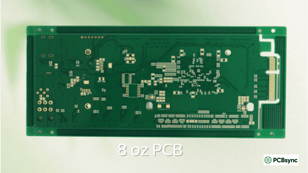
An 8 oz PCB is a printed circuit board manufactured with copper foil weighing 8 ounces per square foot. This measurement translates to a copper thickness of approximately 280 μm (11 mils), making it eight times thicker than the standard 1 oz copper found in typical consumer electronics.
The 8 oz designation places this board type solidly in heavy copper territory. Industry convention generally classifies anything above 3 oz as heavy copper, with extreme heavy copper starting around 10-20 oz. At 8 oz, you’re working with substantial copper mass that fundamentally changes how the board behaves electrically and thermally.
8 oz PCB Technical Specifications
Understanding the numbers helps frame design decisions. Here’s how 8 oz PCB stacks up:
Specification
8 oz PCB Value
Notes
Copper Weight
8 oz/ft²
Per layer
Thickness (metric)
280 μm
Nominal
Thickness (imperial)
11.0 mils
Nominal
Current Multiplier
~4x vs 2 oz
Same trace width
Thermal Conductivity
385 W/m·K
Copper property
Resistivity
1.68 μΩ·cm
At 20°C
Copper Weight Comparison Chart
Context matters when selecting copper weight. Here’s where 8 oz fits in the broader spectrum:
Copper Weight
Thickness (μm)
Thickness (mils)
Classification
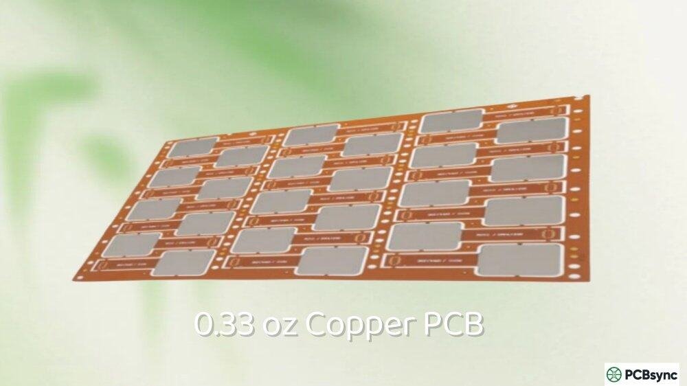
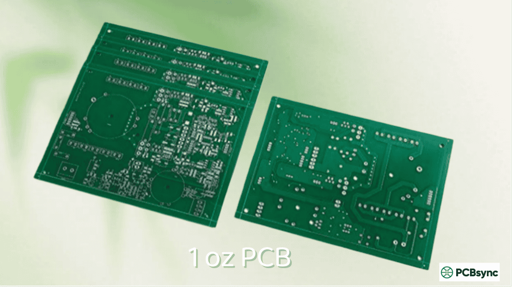
1 oz
35
1.4
Standard
2 oz
70
2.8
Standard
3 oz
105
4.1
Heavy Copper
4 oz
140
5.5
Heavy Copper
6 oz
210
8.3
Heavy Copper
8 oz
280
11.0
Heavy Copper
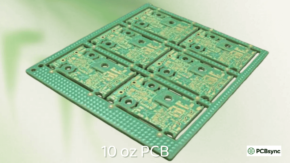
10 oz
350
13.8
Extreme Heavy
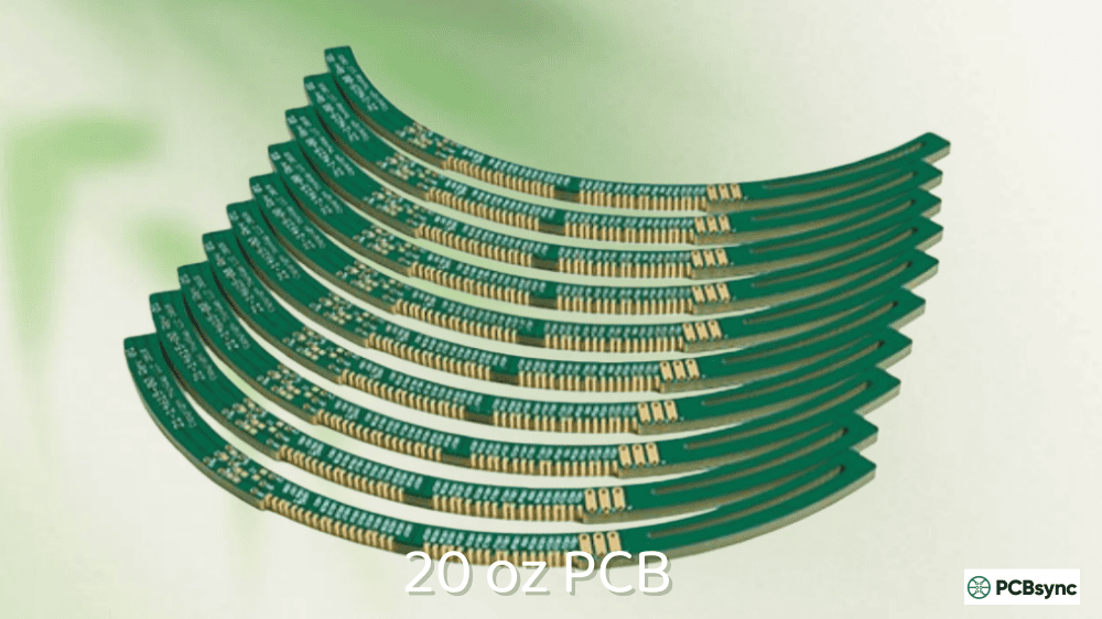
20 oz
700
27.6
Extreme Heavy
Why Engineers Choose 8 oz PCB
The decision to specify 8 oz copper usually comes down to three interrelated factors: current handling, thermal management, and mechanical requirements. Let me break down each one.
High Current Carrying Capability
This is the primary driver for most 8 oz PCB applications. The current-carrying capacity of a PCB trace scales with its cross-sectional area. Double the copper thickness, and you roughly double the ampacity for a given trace width.
For 8 oz copper, a 200 mil (5mm) trace can safely carry 40-55A with a 20°C temperature rise, depending on ambient conditions. Try that with 2 oz copper, and you’d need traces over 500 mils wide, which quickly becomes impractical.
Superior Thermal Dissipation
Copper’s excellent thermal conductivity (385 W/m·K) makes 8 oz PCB an effective heat spreader. The thick copper acts as a built-in heat sink, conducting heat away from hot components and distributing it across a larger area.
I’ve measured temperature reductions of 20-30°C when upgrading power stages from 3 oz to 8 oz copper. In some designs, this eliminates the need for external heat sinks entirely, simplifying assembly and reducing system cost.
Mechanical Strength and Durability
The added copper mass provides significant mechanical benefits. 8 oz PCB boards are substantially more rigid than standard boards, which helps in applications subject to vibration or mechanical stress. The thick plated through-holes also offer better resistance to thermal cycling and mechanical fatigue.
Reduced Trace Widths
Here’s a practical benefit that often gets overlooked. Because 8 oz copper handles more current per unit width, you can use narrower traces for the same current requirement. This frees up board real estate for other routing or allows smaller overall board dimensions.
Based on my project experience and industry trends, these sectors consistently rely on 8 oz PCB technology:
Power Conversion Equipment
Switch-mode power supplies, DC-DC converters, and AC-DC rectifiers in the 2-15 kW range frequently specify 8 oz copper. The combination of high switching currents and thermal demands makes heavy copper essential.
Electric Vehicle Systems
The EV revolution has driven massive growth in 8 oz PCB demand. On-board chargers, motor inverters, battery management systems, and DC fast charging stations all benefit from 8 oz copper construction. Automotive reliability standards further justify the investment.
Industrial Motor Drives
Variable frequency drives, servo amplifiers, and industrial motor controllers operate at sustained high currents in demanding factory environments. 8 oz PCB provides the robustness these applications require.
Renewable Energy Inverters
Solar string inverters and central inverters convert substantial DC power to AC. Wind turbine power converters face similar demands. Both applications leverage 8 oz copper for current handling and thermal management.
Welding Equipment
Industrial welding machines draw enormous currents during operation. 8 oz PCB boards handle the power delivery requirements while surviving the harsh operating conditions.
High-Power LED Systems
Stadium lighting, industrial illumination, and UV curing systems push LED drivers to their limits. 8 oz copper manages both the drive currents and the associated heat generation.
Application Sector
Typical Current Range
Key Requirements
Power Supplies
30-100A
Efficiency, thermal stability
EV Powertrains
50-200A
Reliability, compact size
Motor Drives
40-150A
Sustained operation, durability
Solar Inverters
25-80A
Outdoor environment survival
Welding Systems
100-300A
Extreme current handling
LED Drivers
10-50A
Thermal management
8 oz PCB Design Guidelines
Designing for 8 oz copper requires adjusting your standard practices. These guidelines come from hard-won experience with heavy copper projects.
Trace Width and Spacing Rules
Heavy copper etching produces more undercut than standard copper. The etchant removes copper laterally as it works down through the thickness, resulting in trapezoidal trace cross-sections rather than rectangular ones.
For 8 oz PCB, I recommend minimum trace widths of 12-15 mils (0.30-0.38 mm) and minimum spacing of 14-16 mils. These numbers provide manufacturing margin while remaining achievable at most heavy copper fabricators.
Plating copper into via barrels becomes challenging as copper weight increases. The aspect ratio (board thickness to hole diameter) must remain reasonable for reliable plating. For 8 oz PCB, use larger via diameters than you might in standard designs.
Thermal vias connecting to internal planes should be particularly generous, typically 0.5-0.8mm diameter. These vias transfer heat from surface components to internal copper planes, and larger diameters improve thermal conductivity.
Layer Stackup Strategies
Most 8 oz PCB designs concentrate heavy copper on outer layers, using standard 1-2 oz copper for internal signal layers. This hybrid approach captures the benefits of heavy copper where needed while maintaining signal integrity and manufacturing feasibility.
Common stackup configurations include:
4-layer hybrid: 8 oz outer layers, 1 oz inner signal/power layers 6-layer hybrid: 8 oz outer layers, 2 oz power planes, 1 oz signal layers All heavy: 8 oz on all layers (uncommon, very thick boards)
Thermal Relief Design
Proper thermal reliefs are critical when soldering to 8 oz copper. Without thermal reliefs, the massive copper heat sink prevents solder from reaching proper reflow temperatures, resulting in cold joints or component damage from extended heating.
Design thermal reliefs with 4-6 spokes and adequate air gap. For through-hole components on 8 oz copper, consider thermal reliefs on both top and bottom pads.
Solder Mask Considerations
Solder mask application over 8 oz copper requires attention. The step height between copper and substrate is substantial, and mask coverage can be inconsistent at trace edges. Work with your fabricator on mask specifications, and consider mask-defined pads for fine-pitch components if needed.
Understanding fabrication helps you design more manufacturable boards. Here’s what happens during 8 oz PCB production.
Copper Build-Up Methods
Fabricators achieve 8 oz copper through two primary methods:
Heavy foil lamination: Starting with pre-made 8 oz copper foil laminated to the substrate. This produces uniform thickness but requires specialized material handling.
Electroplating: Starting with lighter base copper (typically 2-3 oz) and plating additional copper to reach target thickness. This allows more flexibility but requires precise process control.
Most shops use a combination approach, starting with 3-4 oz base foil and plating to final thickness. This balances material costs with process reliability.
Pattern Definition and Etching
Creating circuit patterns in 8 oz copper takes significantly longer than standard boards. The extended etching time means more lateral undercutting, which is why design rules are relaxed compared to standard copper.
Modern fabricators use carefully controlled spray etching with continuous monitoring to maintain pattern fidelity. Even so, expect some variation in final trace dimensions.
Drilling and Plating
Drilling through 8 oz copper requires robust drill bits and optimized feed rates. The copper’s mass and thermal conductivity can cause issues with heat buildup during drilling.
Through-hole plating must deposit adequate copper in the barrel while managing the increased surface area of heavy copper boards. Total plating time increases substantially.
Cost Analysis for 8 oz PCB
Budget planning requires understanding cost drivers. Here’s the breakdown for 8 oz PCB projects:
Cost Factor
Impact
Explanation
Raw Copper
High
8x material cost vs 1 oz
Processing Time
High
Extended etching, plating cycles
Equipment Wear
Medium
Heavier duty on production equipment
Yield Loss
Medium
More complex process, lower yields
Specialized Handling
Medium
Heavy panels require care
Testing
Low-Medium
Standard E-test applies
Expect 8 oz PCB pricing to run 2.5-4x standard board costs, depending on complexity and volume. The premium reflects genuine manufacturing challenges, not arbitrary markup.
However, total system cost often favors 8 oz PCB when you factor in eliminated bus bars, reduced heat sink requirements, smaller enclosures, and simplified assembly. Run the full system cost analysis before dismissing heavy copper as too expensive.
8 oz PCB vs Alternative Solutions
Sometimes 8 oz copper isn’t the optimal choice. Here’s how it compares to alternatives:
Solution
Current Capacity
Thermal Performance
Cost
Complexity
Best Application
8 oz PCB
High
Excellent
Medium-High
Medium
Integrated power designs
Insulated Metal Substrate
Medium
Excellent
Medium
Low
LED, single-layer power
Bus Bars + Standard PCB
Very High
Good
Medium
High
100A+ currents
Direct Bonded Copper
High
Outstanding
Very High
High
Extreme power density
Thick Film on Ceramic
Medium
Excellent
High
Medium
High-temperature
Quality and Compliance Standards
When specifying 8 oz PCB, reference these industry standards:
IPC-6012: General PCB qualification and performance requirements, including provisions for heavy copper construction.
IPC-2152: Current carrying capacity standard with guidelines for heavy copper trace sizing.
IPC-A-600: Acceptability criteria for inspecting finished boards, applicable to heavy copper.
UL 796: Safety standard for printed wiring boards, important for power applications.
For automotive applications, ensure your fabricator holds IATF 16949 certification. Aerospace projects may require AS9100 compliance.
Useful Resources for 8 oz PCB Design
These resources support heavy copper design work:
Design Tools and Calculators
Saturn PCB Design Toolkit – Free Windows application for trace width, via current, and thermal calculations
IPC-2152 Calculator Tools – Various online implementations of the current capacity standard
Altium/KiCad Design Rule Templates – Heavy copper rule sets for popular EDA tools
Technical Standards (Available from IPC)
IPC-2152: Standard for Determining Current Carrying Capacity
IPC-6012: Qualification and Performance Specification for Rigid Printed Boards
IPC-2221: Generic Standard on Printed Board Design
Industry Publications
PCB007 Magazine (pcb007.com) – Regular heavy copper coverage
IEEE Xplore – Academic papers on power electronics PCB design
Manufacturer Technical Resources
Request design guides directly from heavy copper PCB fabricators. Their capabilities vary, and their guidelines reflect actual production experience.
Frequently Asked Questions About 8 oz PCB
How much current can an 8 oz PCB trace handle?
Current capacity depends on trace width, acceptable temperature rise, and environmental conditions. As a practical reference, a 250 mil (6.35mm) wide 8 oz trace can carry approximately 50-65A with a 20°C rise above ambient in still air. Always verify using IPC-2152 calculations or thermal simulation for your specific conditions. External airflow significantly increases capacity.
What is the minimum trace width for 8 oz copper?
Most fabricators can reliably produce 12-15 mil (0.30-0.38mm) traces in 8 oz copper. Some specialized shops achieve 10 mils, but this requires careful process control. For production reliability, I recommend designing to 15 mil minimum unless your fabricator confirms tighter capabilities.
Can I use 8 oz copper on internal PCB layers?
Yes, but it’s uncommon and adds complexity. Internal 8 oz copper significantly increases board thickness, affects drilling and registration, and limits fabricator options. Most designs use 8 oz on outer layers only, with standard copper internally. If you need heavy copper throughout, discuss stackup options with potential fabricators early.
How long does 8 oz PCB fabrication take?
Typical lead times run 3-4 weeks for prototype quantities, compared to 1-2 weeks for standard boards. The extended processing time for heavy copper drives this difference. Quick-turn options exist at premium pricing but still require 2+ weeks minimum. Plan your project timeline accordingly.
What’s the difference between 8 oz PCB and thick copper bus bars?
8 oz PCB provides integrated circuit routing, component mounting, and current handling in a single assembly. Bus bars offer higher current capacity (often 200A+) but require separate mounting and connections. For moderate currents (under 100A) where integration matters, 8 oz PCB usually wins. For extreme currents or simple point-to-point connections, bus bars may be more practical.
Making Your 8 oz PCB Decision
Selecting 8 oz copper comes down to matching capabilities with requirements. Choose 8 oz PCB when your application needs 30-100A current handling in compact form factor, demands integrated thermal management, must withstand harsh environments, and benefits from manufacturing simplification over bus bar approaches.
Consider alternatives when currents exceed 150A consistently, thermal requirements point toward IMS or DBC substrates, budget constraints are severe, or simpler solutions adequately meet requirements.
The 8 oz threshold represents capable heavy copper that remains accessible from established fabricators worldwide. For power electronics designers, it’s often the practical choice that balances performance against manufacturing complexity and cost.
Start your fabricator conversations early in the design process. Their specific capabilities and design guidance will shape your final layout decisions, and early collaboration prevents costly respins later.
Inquire: Call 0086-755-23203480, or reach out via the form below/your sales contact to discuss our design, manufacturing, and assembly capabilities.
Quote: Email your PCB files to Sales@pcbsync.com (Preferred for large files) or submit online. We will contact you promptly. Please ensure your email is correct.
Notes: For PCB fabrication, we require PCB design file in Gerber RS-274X format (most preferred), *.PCB/DDB (Protel, inform your program version) format or *.BRD (Eagle) format. For PCB assembly, we require PCB design file in above mentioned format, drilling file and BOM. Click to download BOM template To avoid file missing, please include all files into one folder and compress it into .zip or .rar format.


