Inquire: Call 0086-755-23203480, or reach out via the form below/your sales contact to discuss our design, manufacturing, and assembly capabilities.
Quote: Email your PCB files to Sales@pcbsync.com (Preferred for large files) or submit online. We will contact you promptly. Please ensure your email is correct.
Notes: For PCB fabrication, we require PCB design file in Gerber RS-274X format (most preferred), *.PCB/DDB (Protel, inform your program version) format or *.BRD (Eagle) format. For PCB assembly, we require PCB design file in above mentioned format, drilling file and BOM. Click to download BOM template To avoid file missing, please include all files into one folder and compress it into .zip or .rar format.
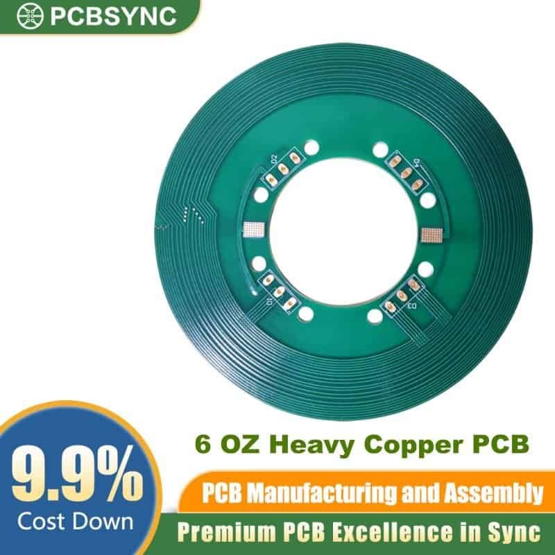
I’ve spent over a decade working with power electronics, and if there’s one thing I’ve learned, it’s that standard 1 oz PCBs simply don’t cut it when you’re pushing serious current. That’s where 6 oz PCB technology comes in. Whether you’re designing EV battery management systems, industrial motor drives, or aerospace power distribution units, understanding heavy copper boards is essential for any engineer working in high-power applications.
In this guide, I’ll walk you through everything you need to know about 6 oz copper PCB design, from basic specifications to practical design rules I’ve learned through hard-won experience.
A 6 oz PCB refers to a printed circuit board with copper layers weighing 6 ounces per square foot. To put that in perspective, the copper layer thickness works out to approximately 210 µm (8.2 mils), which is six times thicker than the standard 1 oz copper found on most consumer electronics boards.
This might seem like a minor detail, but the difference is massive in practice. When you’re dealing with currents of 20, 30, or even 50+ amps, that extra copper mass becomes your best friend for two critical reasons: current carrying capacity and thermal management.
Why Engineers Choose 6 oz PCB for High-Power Designs
After years of designing power electronics, I can tell you that choosing 6 oz copper isn’t about overkill. It’s about solving real engineering problems that standard boards simply cannot address.
Superior Current Carrying Capacity
The primary reason to use a 6 oz PCB is straightforward: thicker copper means lower resistance, which means you can push more current through narrower traces without overheating.
Here’s a practical example. Using IPC-2221 guidelines, a 1 oz copper trace carrying 5A requires approximately 0.2 inches (5 mm) of width to keep temperature rise under 10°C. With 6 oz copper, that same 5A current only needs about 0.03 inches (0.76 mm) of trace width. That’s a massive reduction in board real estate.
Thermal Management Benefits
Heat kills electronics. Full stop. The thick copper layers in a 6 oz PCB act as integrated heat spreaders, pulling thermal energy away from hot components like MOSFETs, IGBTs, and power transistors. I’ve seen designs where switching from 2 oz to 6 oz copper reduced hot spot temperatures by 40-60°C without any additional heatsinking.
The thermal conductivity of copper (401 W/m·K) is roughly 10 times better than the FR4 substrate material beneath it. By increasing your copper mass, you’re essentially building a heat sink directly into your PCB.
Mechanical Strength and Reliability
6 oz copper boards are significantly more robust than their thin-copper counterparts. The added copper mass provides better resistance to thermal cycling stress, reduces the risk of trace cracking, and improves plated through-hole (PTH) reliability. In automotive and aerospace applications where vibration and temperature swings are constant, this mechanical advantage is critical.
Understanding how 6 oz PCB compares to other copper weights helps you make informed design decisions. Here’s a comprehensive breakdown:
Copper Weight
Thickness (mils)
Thickness (µm)
Min Trace/Space (mils)
Typical Current Range
Best Applications
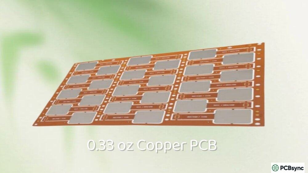
0.5 oz
0.7
17.5
4/4
< 1A
Signal routing, consumer electronics
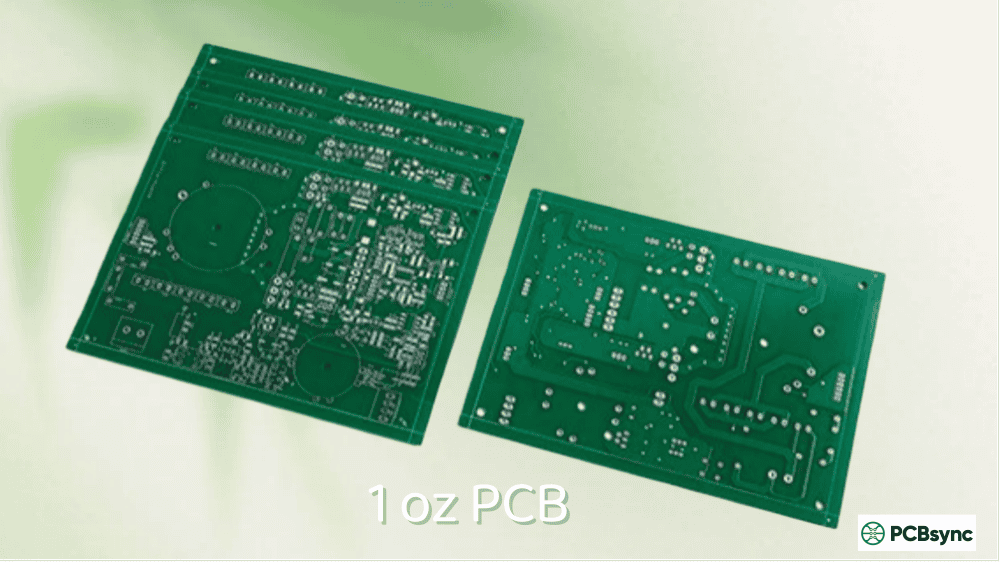
1 oz
1.37
35
5/5
1-3A
Standard electronics, LED drivers
2 oz
2.74
70
8/8
3-10A
Power supplies, motor drivers
3 oz
4.11
105
10/10
10-15A
Industrial controls, UPS systems
4 oz
5.48
140
12/12
15-25A
Heavy-duty power electronics
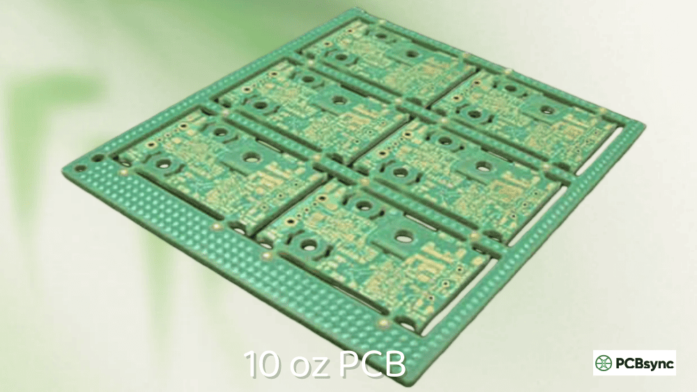
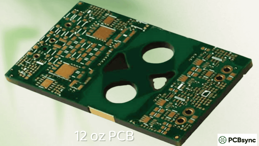
6 oz
8.22
210
13/13
25-50A+
EV systems, aerospace, high-power inverters
6 oz PCB Design Guidelines
Designing with heavy copper requires different considerations than standard PCB work. Here are the essential rules I follow on every 6 oz PCB project.
Trace Width and Spacing Requirements
The etching process for thick copper is more aggressive, which means you need wider traces and larger gaps between conductors. For 6 oz copper, the industry standard minimum is 13 mils (0.33 mm) for both trace width and spacing.
However, I always recommend adding margin. If your design allows 15-20 mil spacing, use it. The pcb manufacturing yield improves significantly, and you’ll have fewer headaches during fabrication.
Copper Fill and Resin Considerations
One critical design rule that newer engineers often miss: copper fill levels with resin materials must exceed 75%. If you don’t maintain adequate copper coverage, you risk delamination during thermal cycling. This happens because uneven copper distribution creates differential stress during temperature changes.
Distribute your copper as evenly as possible across each layer. If you have dense copper on one area and sparse coverage elsewhere, add copper pour (connected to ground or power) to balance the distribution.
Solder Mask Thickness
Standard solder mask applications won’t cut it with 6 oz copper. The copper edges create sharp step-heights that thin solder mask can’t adequately cover. Specify a minimum solder mask thickness of 0.25 mm, and work with your manufacturer to determine if multiple print passes are necessary.
I’ve seen boards where exposed copper edges caused shorts during assembly. Don’t let that happen to your design.
Via Design for Heavy Copper
Vias in 6 oz PCB require special attention. Standard vias might not survive the thermal and current stress of high-power applications. Consider these guidelines:
Via sizing: Use larger drill sizes (12+ mils) with appropriate annular rings to ensure adequate copper plating in the barrel.
Thermal vias: Place thermal vias beneath heat-generating components. Use via arrays rather than single vias to distribute heat effectively.
Via filling: For high-reliability applications, specify via filling or capping to prevent solder wicking and improve thermal conductivity.
Layer Stackup Recommendations
When designing multilayer 6 oz PCB stackups, maintain balance. If you use 6 oz copper on the top layer, use 6 oz on the bottom layer as well. An unbalanced stackup leads to board warping during reflow soldering.
A typical 4-layer stackup for high-power applications might look like this:
Heavy copper PCBs aren’t for every project. They cost more and require specialized manufacturing capabilities. But for certain applications, 6 oz PCB technology is the only viable solution.
Electric Vehicle Power Electronics
The EV industry has driven enormous growth in heavy copper PCB demand. Battery management systems (BMS), onboard chargers, DC-DC converters, and motor inverters all require boards that can handle 100+ amps while managing significant thermal loads.
In EV battery packs, 6 oz copper PCBs handle current flows between cells, ensuring safe and efficient power distribution. The thermal management benefits are particularly important given the confined spaces and high ambient temperatures inside vehicle battery enclosures.
Automotive Electronics
Beyond EVs, traditional automotive applications increasingly rely on heavy copper boards. Engine control units, lighting systems, and infotainment power supplies all benefit from improved current handling and thermal performance.
The automotive environment is brutal: temperatures from -40°C to +125°C, constant vibration, and zero tolerance for failure. 6 oz PCB construction provides the ruggedness these applications demand.
Aerospace and Defense
Military and aerospace systems require exceptional reliability under extreme conditions. Heavy copper PCBs are standard in radar systems, avionics, satellite communications, and power distribution for aircraft and spacecraft.
These applications often specify additional testing requirements including thermal cycling, vibration testing, and high-voltage breakdown verification.
Industrial Power Systems
Motor drives, welding equipment, industrial automation, and power inverters all benefit from 6 oz copper construction. Industrial environments often expose electronics to harsh conditions including dust, moisture, and temperature extremes.
Renewable Energy
Solar inverters, wind turbine controllers, and energy storage systems require efficient power conversion at high current levels. 6 oz PCB technology enables compact designs that maximize energy conversion efficiency while minimizing thermal losses.
Manufacturing Considerations for 6 oz PCB
Not every PCB fabricator can produce quality 6 oz copper boards. When selecting a manufacturer, consider these factors:
Fabricator Capabilities
Verify that your chosen manufacturer has documented experience with heavy copper. Key questions to ask include:
What’s their maximum copper weight capability?
Do they have specialized etching and plating equipment?
Can they provide references for similar projects?
What certifications do they hold (ISO 9001, AS9100, IATF 16949)?
Extended Lead Times
Heavy copper boards require longer processing times. The thicker copper takes longer to etch, and multiple plating and lamination cycles may be necessary. Plan for 2-3 weeks additional lead time compared to standard boards.
Cost Factors
6 oz PCB boards cost more than standard construction. The price premium comes from:
Higher raw material costs (more copper)
Longer processing times
Lower manufacturing yields
Specialized equipment requirements
For prototypes, expect 40-60% higher costs. Volume pricing reduces the differential but never eliminates it entirely.
Surface Finish Options for 6 oz Copper PCB
Surface finish selection impacts both solderability and long-term reliability. For 6 oz copper applications, I typically recommend:
ENIG (Electroless Nickel Immersion Gold)
ENIG provides excellent corrosion protection and solderability. The nickel barrier prevents copper dissolution during soldering, which is particularly important for thick copper where more thermal mass means longer reflow times.
HASL (Hot Air Solder Leveling)
Lead-free HASL remains a cost-effective option for power electronics where surface flatness isn’t critical. It provides good shelf life and excellent solderability.
OSP (Organic Solderability Preservative)
OSP offers the lowest cost but limited shelf life. Use this finish only when boards will be assembled quickly after fabrication.
Common 6 oz PCB Design Mistakes to Avoid
Having reviewed hundreds of heavy copper designs, I see certain mistakes repeatedly. Learn from others’ errors:
Underestimating thermal management: Even with 6 oz copper, poor thermal design leads to hot spots. Always simulate thermal performance before committing to production.
Ignoring via current limits: Don’t assume vias can carry unlimited current. Calculate via requirements using IPC-2152 guidelines.
Insufficient copper balance: Uneven copper distribution causes warping. Use copper pour to balance coverage across each layer.
Wrong surface finish: Selecting the wrong finish leads to soldering problems. Match your finish to your assembly process and application requirements.
Skimping on solder mask: Thin solder mask leads to exposed copper edges and potential shorts. Specify adequate thickness.
Useful Resources and Tools
Here are the tools and references I use regularly for 6 oz PCB design:
DigiKey Trace Width Calculator: Online tool using IPC-2221 formulas (digikey.com)
Sierra Circuits IPC-2152 Calculator: Advanced calculator with modification factors (protoexpress.com)
CircuitDigest Calculator: Simple online tool with design recommendations (circuitdigest.com)
Industry Standards
IPC-2221B: Generic standard on printed board design
IPC-2152: Standard for determining current-carrying capacity in printed board design
IPC-6012: Qualification and performance specification for rigid printed boards
Design Software
Altium Designer: Full-featured PCB design with excellent heavy copper support
KiCad: Open-source option with custom design rules for heavy copper
Cadence OrCAD: Industry standard with IPC-2221 integration
Frequently Asked Questions About 6 oz PCB
What current can a 6 oz copper PCB handle?
A 6 oz PCB can handle significantly higher currents than standard boards. For a 100 mil wide external trace with 10°C temperature rise, 6 oz copper can carry approximately 25-30 amps. The exact value depends on trace geometry, ambient temperature, and surrounding copper coverage. Always use an IPC-2152 compliant calculator for accurate current capacity estimation in your specific design.
Is 6 oz copper PCB more expensive than standard boards?
Yes, 6 oz copper PCBs typically cost 40-60% more than equivalent 1-2 oz boards for prototype quantities. The premium decreases with volume but never disappears entirely. The higher cost reflects increased raw material usage, longer processing times, and lower manufacturing yields. However, the improved performance and reliability often justify the investment, particularly in applications where board failure would be catastrophic or expensive.
Can I use SMD components on 6 oz copper PCB?
Absolutely. Both surface mount and through-hole components work with 6 oz copper boards. However, the increased copper mass requires adjustments to your soldering process. The thick copper acts as a heat sink during reflow, potentially causing cold solder joints if profiles aren’t optimized. Work closely with your assembly partner to develop appropriate thermal profiles for your specific board design.
How does 6 oz copper affect PCB impedance?
The thick copper layer significantly impacts impedance calculations. With six times more copper thickness than standard boards, trace geometry for controlled impedance designs changes substantially. Use accurate modeling tools that account for the specific trace thickness, and work with your fabricator to verify impedance targets can be achieved with their manufacturing tolerances.
What’s the typical lead time for 6 oz copper PCB fabrication?
Expect lead times of 3-4 weeks for standard 6 oz copper boards, compared to 1-2 weeks for conventional PCBs. Rush services are available from some manufacturers at premium pricing. The extended timeline reflects the additional processing steps required for thick copper etching, plating, and lamination. For prototypes, factor this timeline into your project schedule from the start.
Conclusion
6 oz copper PCB technology has become indispensable for modern high-power electronics. From electric vehicles to aerospace systems, heavy copper boards enable designs that would be impossible with standard construction. While they require specialized design knowledge and careful manufacturing partner selection, the performance benefits are substantial.
The key to successful 6 oz PCB design lies in understanding the unique requirements: wider traces and spacing, careful thermal management, balanced copper distribution, and appropriate surface finish selection. Follow the guidelines in this article, use the right calculation tools, and work with experienced fabricators to bring your high-power designs to life.
If you’re transitioning from standard PCB design to heavy copper work, start with a simple project to learn the manufacturing quirks before tackling your most complex design. The learning curve is manageable, and the capabilities you gain will open new possibilities for your power electronics projects.
Inquire: Call 0086-755-23203480, or reach out via the form below/your sales contact to discuss our design, manufacturing, and assembly capabilities.
Quote: Email your PCB files to Sales@pcbsync.com (Preferred for large files) or submit online. We will contact you promptly. Please ensure your email is correct.
Notes: For PCB fabrication, we require PCB design file in Gerber RS-274X format (most preferred), *.PCB/DDB (Protel, inform your program version) format or *.BRD (Eagle) format. For PCB assembly, we require PCB design file in above mentioned format, drilling file and BOM. Click to download BOM template To avoid file missing, please include all files into one folder and compress it into .zip or .rar format.


