Inquire: Call 0086-755-23203480, or reach out via the form below/your sales contact to discuss our design, manufacturing, and assembly capabilities.
Quote: Email your PCB files to Sales@pcbsync.com (Preferred for large files) or submit online. We will contact you promptly. Please ensure your email is correct.
Notes: For PCB fabrication, we require PCB design file in Gerber RS-274X format (most preferred), *.PCB/DDB (Protel, inform your program version) format or *.BRD (Eagle) format. For PCB assembly, we require PCB design file in above mentioned format, drilling file and BOM. Click to download BOM template To avoid file missing, please include all files into one folder and compress it into .zip or .rar format.
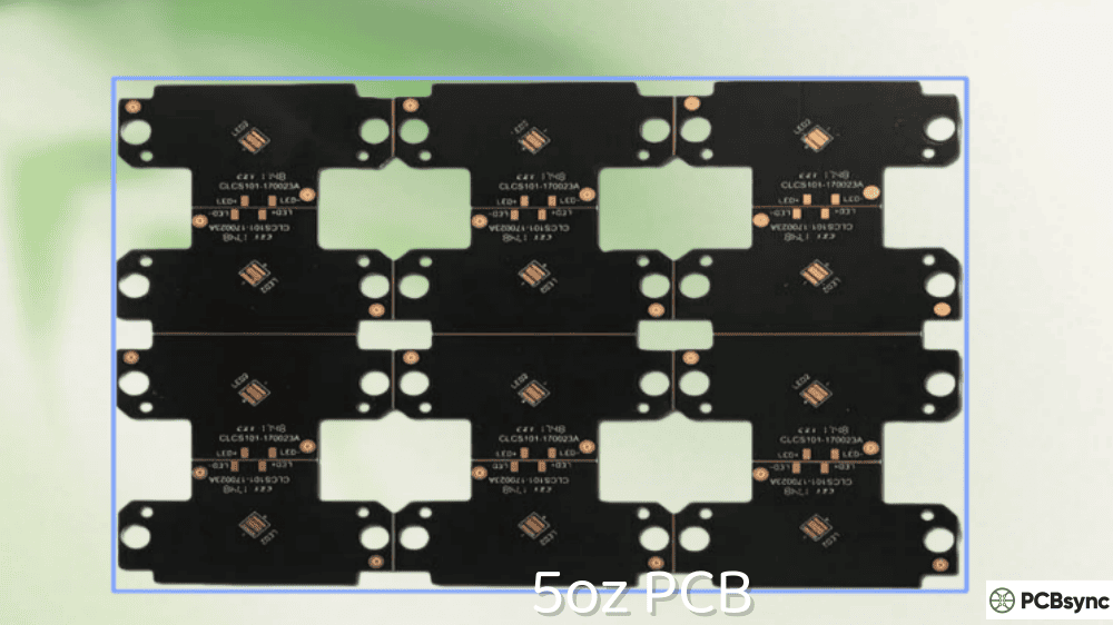
The 5 oz PCB sits in an interesting position in the heavy copper spectrum. It’s not as commonly discussed as 4 oz or 6 oz boards, but for certain applications, it offers the perfect balance between current capacity, thermal performance, and manufacturing complexity. This guide covers everything you need to know about designing with 5 oz copper—from basic specifications to real-world implementation strategies that actually work in production.
What is 5 oz PCB? Understanding Heavy Copper Specifications
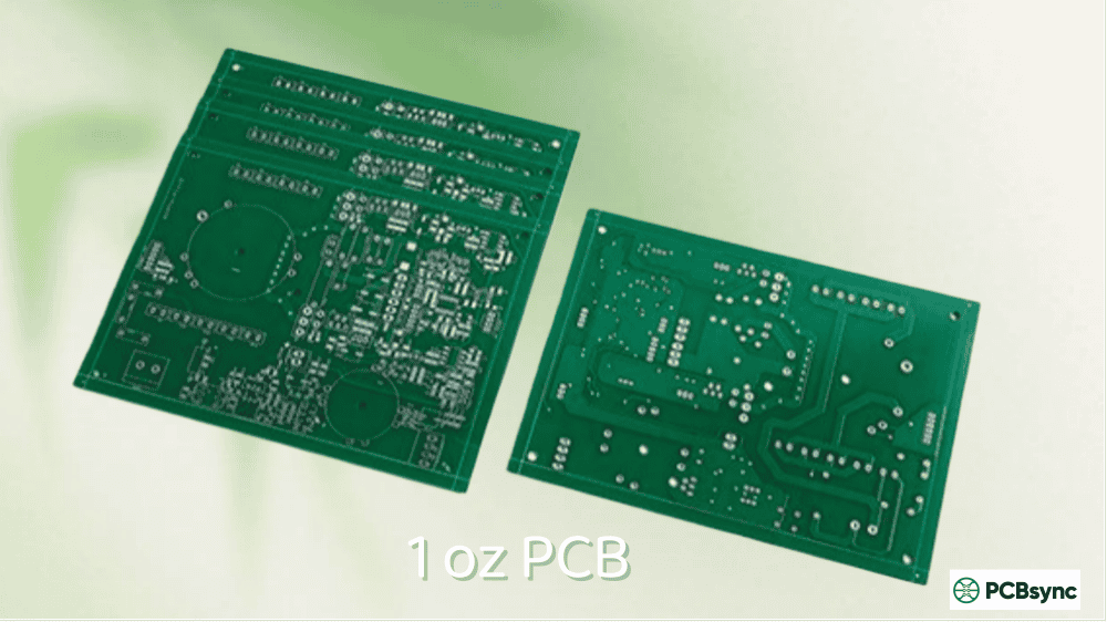
A 5 oz PCB refers to a printed circuit board with copper layers weighing 5 ounces per square foot. In terms of actual thickness, this translates to approximately 175 microns (0.175mm or 6.85 mils) of copper on each conductive layer. That’s five times thicker than the standard 1 oz copper found in consumer electronics and represents serious heavy copper territory.
The “ounce” measurement system comes from the weight of copper foil that would cover one square foot of board area. It’s an old convention from early PCB manufacturing that stuck around because it’s actually quite practical for specifying copper weight during ordering and fabrication. When you tell a fab house you need 5 oz copper, there’s no ambiguity about what you’re asking for.
Table 1: Complete Copper Weight to Thickness Conversion Chart
Where Does 5 oz PCB Fit in the Heavy Copper Spectrum?
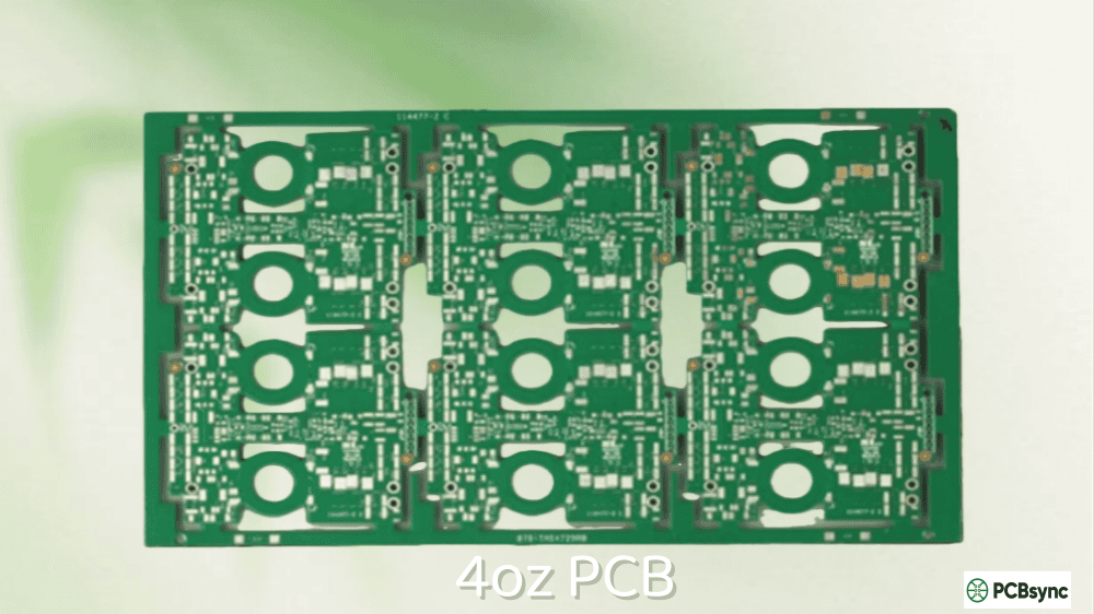
In the PCB industry, anything 3 oz and above is typically classified as “heavy copper.” The 5 oz PCB falls squarely in the middle of this range, which gives it some unique advantages. It provides significantly more current capacity than 4 oz boards while being easier to manufacture than 6 oz or higher weights.
I’ve found that 5 oz copper hits a practical sweet spot for applications that push beyond 4 oz capabilities but don’t justify the additional cost and manufacturing complexity of 6 oz boards. The incremental improvement from 4 oz to 5 oz is often enough to provide the thermal and electrical margin needed without over-engineering the solution.
Key Benefits of 5 oz PCB for High-Power Applications
Choosing 5 oz copper PCB over standard options brings several significant advantages. Let me walk through the ones that matter most in real-world applications.
Superior Current Carrying Capacity for 5 oz PCB
The primary reason engineers choose 5 oz PCB is current handling capability. According to IPC-2152 calculations, a 5 oz copper trace can safely carry approximately 25% more current than a 4 oz trace of the same width at equivalent temperature rise. For a 10mm wide external trace with a 10°C rise above ambient, you’re looking at roughly 85-90 amps capacity.
On a recent traction inverter project, we needed to route 75A continuous through a relatively constrained board area. With 4 oz copper, we would have needed 12mm traces and were running tight on space. Moving to 5 oz let us drop to 10mm traces while gaining additional thermal headroom—a win on both fronts.
Table 2: Current Capacity Comparison by Copper Weight (10°C Rise, External Layer)
Trace Width
2 oz
4 oz
5 oz
6 oz
5mm
~14A
~35A
~43A
~52A
10mm
~30A
~70A
~87A
~105A
15mm
~45A
~100A
~125A
~150A
20mm
~58A
~130A
~160A
~195A
Note: Values are approximate estimates based on IPC-2152. Always verify with proper calculations for your specific design conditions.
Enhanced Thermal Management with 5 oz Copper PCB
Thermal performance is where 5 oz PCB really demonstrates its value. Copper’s thermal conductivity (approximately 400 W/m·K) is roughly 1000 times better than FR-4 substrate. When you increase copper thickness by 25% going from 4 oz to 5 oz, you’re adding substantial thermal mass and heat spreading capability.
In practical terms, I’ve measured temperature reductions of 8-12°C on power semiconductor packages just by upgrading from 4 oz to 5 oz copper on the thermal plane, with no other design changes. That extra margin can be the difference between needing active cooling and getting by with natural convection.
Improved Mechanical Strength and Reliability
The additional copper mass in a 5 oz PCB provides better mechanical support for heavy components and connectors. The thicker copper walls in plated through-holes resist thermal cycling stress more effectively, reducing the risk of barrel cracks in high-reliability applications.
This becomes particularly important in applications with significant temperature swings. Aerospace systems, for example, may see temperature excursions from -40°C to +85°C repeatedly. The mechanical robustness of 5 oz copper helps maintain via integrity through thousands of thermal cycles.
Potential for Reduced Layer Count with 5 oz PCB
One often-overlooked benefit of 5 oz copper PCB is the potential to reduce layer count. Instead of using multiple parallel 2 oz layers to achieve the required current capacity, a single 5 oz layer can often do the job. This simplifies the stackup, reduces board thickness, and can actually lower total cost despite the higher per-layer expense.
5 oz PCB Applications: Where Heavy Copper Delivers Value
Not every project needs 5 oz PCB technology, but in the right applications, it’s the optimal choice. Here are the industries and use cases where I consistently see 5 oz copper providing real benefits.
Industrial Power Electronics and Motor Control
Industrial applications are the bread and butter of 5 oz PCB usage. Variable frequency drives (VFDs), servo controllers, and power converters for manufacturing equipment routinely handle 30-80A continuous current in elevated ambient temperatures. The thermal margin provided by 5 oz copper becomes essential for reliable 24/7 operation.
Motor controllers and variable frequency drives (VFDs)
Industrial power supplies and UPS systems
Welding equipment power electronics
CNC machine servo amplifiers
Industrial automation control panels
Electric Vehicle and Traction Systems
The EV revolution has driven significant demand for heavy copper PCBs, including 5 oz PCB boards. Battery management systems handling 100A+ charge/discharge currents, onboard chargers, and DC-DC converters all benefit from the enhanced current and thermal capacity.
Battery Management Systems (BMS) for EVs
Onboard chargers (OBC) and DC-DC converters
Traction inverters for electric motors
Charging station power modules
Railway traction converters
Renewable Energy and Power Conversion
Solar inverters, wind turbine power electronics, and energy storage systems represent growing markets for 5 oz PCB technology. These applications demand high efficiency and long-term reliability, often in harsh environmental conditions.
Grid-tie solar inverters
Battery energy storage system (BESS) power modules
Wind turbine power converters
Solar charge controllers
Table 3: 5 oz PCB Application Summary by Industry
Industry Sector
Typical Current Range
Key Requirements
Industrial Power
30-100A
Continuous operation, heat
EV/Traction
50-200A+
Thermal cycling, reliability
Renewable Energy
40-150A
Long-term reliability, efficiency
Aerospace/Defense
20-80A
Extreme temps, vibration
Medical Equipment
15-60A
Safety, reliability
5 oz PCB vs 4 oz vs 6 oz: Choosing the Right Copper Weight
One of the most common questions I get is: “Should I use 4 oz, 5 oz PCB, or go straight to 6 oz?” The answer depends on your specific requirements, and understanding the tradeoffs helps make the right decision.
Table 4: Heavy Copper PCB Comparison (4 oz vs 5 oz vs 6 oz)
Specification
4 oz PCB
5 oz PCB
6 oz PCB
Thickness (mils)
5.48
6.85
8.22
Thickness (µm)
140
175
210
Min Trace Width
10-12 mils
12-14 mils
14-16 mils
Min Spacing
12-16 mils
14-18 mils
18-20 mils
Relative Cost
1.5-2x standard
1.8-2.5x standard
2-3x standard
Lead Time
2-3 weeks
2.5-4 weeks
3-5 weeks
Fab Availability
Most heavy Cu fabs
Many heavy Cu fabs
Specialty fabs
When to Choose 5 oz PCB Over 4 oz
Consider upgrading to 5 oz PCB when:
Your current 4 oz design runs at 80%+ of theoretical current capacity
Thermal imaging shows hot spots within 15°C of component limits
You need 20-30% more current capacity but want to keep similar trace widths
The application involves significant thermal cycling (automotive, aerospace)
Board real estate is constrained and you can’t widen traces further
When 6 oz PCB Makes More Sense Than 5 oz
Jump to 6 oz copper instead of 5 oz PCB when:
Current requirements exceed 100A continuous per trace
5 oz PCB Design Guide: Best Practices for Engineers
Designing with 5 oz copper requires specific considerations beyond standard PCB layout. The manufacturing process differences and thermal characteristics demand adapted design rules. Here’s what works in production.
Trace Width and Spacing Requirements for 5 oz PCB
Thicker copper requires wider minimum trace widths and larger spacing between features. For 5 oz PCB, most manufacturers specify minimum trace widths of 12-14 mils (0.30-0.35mm) and minimum spacing of 14-18 mils (0.35-0.45mm). These requirements are significantly larger than standard 1 oz boards because the longer etching time causes more lateral undercutting.
Table 5: Minimum Trace/Space Requirements by Copper Weight
Copper Weight
Min Trace (mils)
Min Space (mils)
Etch Factor
1 oz
4-5
4-5
0.0015″
2 oz
5-6
6-8
0.0025″
3 oz
8-10
9-12
0.003″
4 oz
10-12
12-16
0.0035″
5 oz
12-14
14-18
0.004″
6 oz
14-16
18-20
0.0045″
Important: Always verify specific capabilities with your PCB manufacturer. These values vary between fabrication houses.
Layer Stackup Design for 5 oz Copper PCB
A well-designed stackup is critical for 5 oz PCB success. The general approach is to use 5 oz copper on layers carrying high current while keeping inner signal layers at lower weights. This balances current capacity with routing density and helps prevent warping.
For a typical 4-layer power board with 5 oz copper, I recommend: Layer 1 (Top) – 5 oz for power traces and thermal planes; Layer 2 – 1-2 oz for ground plane; Layer 3 – 1-2 oz for signal routing; Layer 4 (Bottom) – 5 oz for power return and additional thermal mass. Maintaining symmetry (same copper weight on mirrored layers) prevents board warping during thermal cycling.
Thermal Management Strategies for 5 oz PCB Designs
Even with the excellent thermal properties of 5 oz copper, proper thermal design remains essential. Here are the strategies I use consistently:
Thermal via arrays: Place arrays of vias (0.3-0.5mm diameter, 1-1.5mm pitch) under power components to transfer heat to inner planes or the opposite board side.
Copper flood fills: Fill unused board area with copper connected to ground or power. This adds thermal mass and spreading capability even in non-critical areas.
Component placement: Position heat-generating components to maximize copper area beneath them and ensure adequate airflow paths if convection cooling is used.
Thermal relief considerations: While direct connections provide better thermal performance, thermal reliefs may be necessary for large copper areas to enable proper soldering.
Via Design for High-Current 5 oz PCB Applications
Standard vias become a current bottleneck in 5 oz PCB designs. The typical 1 oz copper plating in via walls may not handle the current density or thermal stress that 5 oz board layers experience. For 5 oz designs:
Use minimum via diameter of 0.35mm (14 mils) for current-carrying vias
Specify 2-2.5 oz minimum copper plating in via walls
Calculate via current capacity at 2-3A per standard via; use multiple paralleled vias for high-current paths
Consider filled and capped vias for components with thermal pads
Use large via pads to accommodate 5 oz copper registration tolerances
Material Selection for 5 oz Copper PCB
Substrate material choice affects both thermal performance and reliability of 5 oz PCB designs. Standard FR-4 (Tg 130-140°C) works for moderate applications, but high-Tg materials (170-180°C) are recommended for demanding environments. For the most extreme applications, polyimide substrates handle continuous operation at 250°C.
5 oz PCB Manufacturing: What Engineers Need to Know
Manufacturing 5 oz copper PCB is more challenging than standard boards, and not every fabricator handles it well. Understanding the process challenges helps you set realistic expectations and select the right manufacturing partner.
Common Manufacturing Challenges with 5 oz PCB
The extended etching time required for 5 oz copper creates several manufacturing challenges. Undercutting becomes more pronounced as etchant works through the thick copper, potentially causing trace width variation. Lamination must be carefully controlled to prevent inner layer misregistration. Via plating requires special attention to achieve void-free fill with adequate wall thickness.
Lead times for 5 oz boards typically run 2.5-4 weeks for prototypes—significantly longer than standard boards. Production quantities may take 4-6 weeks depending on complexity. Build these timelines into your project schedule from the start.
How to Select a 5 oz PCB Manufacturer
When evaluating fabricators for 5 oz PCB production, look for these qualifications:
Demonstrated heavy copper experience (ask for specific 5 oz case studies)
ISO 9001 certification and UL approval for the copper weights you need
Saturn PCB Design Toolkit: Free downloadable suite with comprehensive PCB calculations
CircuitCalculator.com: circuitcalculator.com/wordpress/?p=25/ (trace width and current)
Industry Standards for Heavy Copper PCB Design
IPC-2152: Standard for Determining Current Carrying Capacity in PCBs (primary reference for current calculations)
IPC-2221: Generic Standard on Printed Board Design (general design guidelines)
IPC-6012: Qualification and Performance Specification for Rigid PCBs
IPC-4101: Specification for Base Materials for Rigid and Multilayer PCBs
MIL-PRF-31032: Military specification for high-reliability PCBs (relevant for aerospace/defense)
Frequently Asked Questions About 5 oz PCB
1. What is the exact thickness of 5 oz copper PCB?
A 5 oz PCB has copper layers approximately 175 microns (0.175mm or 6.85 mils) thick per layer. This is based on spreading 5 ounces of copper evenly over one square foot of board area. For a board with 5 oz copper on both outer layers, the total copper thickness would be 350 µm (0.35mm) plus substrate and any inner layer copper.
2. How much current can a 5 oz copper trace handle?
Current capacity depends on trace width, acceptable temperature rise, and whether the trace is internal or external. For a 10mm wide external trace on 5 oz copper with a 10°C temperature rise, expect approximately 85-90A capacity. Internal traces have roughly 50% the capacity due to poorer heat dissipation. Always verify with IPC-2152 calculations for your specific conditions and add appropriate safety margins.
3. Is 5 oz PCB significantly more expensive than 4 oz?
Yes, 5 oz PCB typically costs 15-30% more than equivalent 4 oz boards. The premium comes from increased material cost, longer processing times, and tighter process control requirements. However, the cost difference often becomes less significant in production volumes, and the improved performance may eliminate the need for external heatsinks or additional cooling, potentially reducing system-level cost.
4. What are the minimum trace width and spacing for 5 oz copper?
Most fabricators specify minimum trace width of 12-14 mils (0.30-0.35mm) and minimum spacing of 14-18 mils (0.35-0.45mm) for 5 oz PCB. These are larger than 4 oz requirements (10-12/12-16 mils) because thicker copper needs longer etching time, causing more lateral undercutting. Always confirm specific limits with your chosen manufacturer, as capabilities vary.
5. When should I choose 5 oz over 4 oz or 6 oz copper?
Choose 5 oz PCB when your 4 oz design runs near its current or thermal limits but 6 oz would be overkill. It’s ideal when you need 20-30% more current capacity than 4 oz provides, want better thermal margin without the full jump to 6 oz, or face board space constraints that prevent widening traces. If you need more than 100A per trace or operate in extreme thermal environments, move directly to 6 oz or higher.
Conclusion: Making the Most of 5 oz PCB Technology
5 oz PCB occupies a valuable middle ground in the heavy copper spectrum. For applications that push beyond 4 oz capabilities but don’t require the full weight of 6 oz boards, it provides an optimal balance of current capacity, thermal performance, and PCB manufacturing practicality.
The key to successful 5 oz copper implementation lies in understanding its specific design requirements. Adjust your trace widths and spacing, design appropriate layer stackups, plan thermal management carefully, and work with experienced fabricators who understand heavy copper manufacturing. Don’t simply scale up a design meant for standard copper—adapt it specifically for 5 oz characteristics.
As power density continues increasing across industries—from EVs to industrial automation to renewable energy systems—5 oz PCB technology will remain an essential tool in the power electronics designer’s toolkit. Master these design principles, and you’ll be well-equipped to tackle demanding high-current applications where standard copper simply won’t suffice.
Inquire: Call 0086-755-23203480, or reach out via the form below/your sales contact to discuss our design, manufacturing, and assembly capabilities.
Quote: Email your PCB files to Sales@pcbsync.com (Preferred for large files) or submit online. We will contact you promptly. Please ensure your email is correct.
Notes: For PCB fabrication, we require PCB design file in Gerber RS-274X format (most preferred), *.PCB/DDB (Protel, inform your program version) format or *.BRD (Eagle) format. For PCB assembly, we require PCB design file in above mentioned format, drilling file and BOM. Click to download BOM template To avoid file missing, please include all files into one folder and compress it into .zip or .rar format.


