Inquire: Call 0086-755-23203480, or reach out via the form below/your sales contact to discuss our design, manufacturing, and assembly capabilities.
Quote: Email your PCB files to Sales@pcbsync.com (Preferred for large files) or submit online. We will contact you promptly. Please ensure your email is correct.
Notes: For PCB fabrication, we require PCB design file in Gerber RS-274X format (most preferred), *.PCB/DDB (Protel, inform your program version) format or *.BRD (Eagle) format. For PCB assembly, we require PCB design file in above mentioned format, drilling file and BOM. Click to download BOM template To avoid file missing, please include all files into one folder and compress it into .zip or .rar format.
If you’ve spent any time on an SMT production line, you’ve probably heard the statistic: somewhere between 60% and 70% of all PCB assembly defects trace back to the solder paste printing process. After 15 years of troubleshooting failed boards and chasing down intermittent connections, I can tell you that number isn’t exaggerated. It’s actually conservative on some lines.
The solder paste printing step seems deceptively simple. Squeegee pushes paste through stencil apertures onto pads. Done. But anyone who’s dealt with tombstoning on 0201 components, head-in-pillow defects on BGAs, or random bridging on fine-pitch QFPs knows that getting consistent paste deposition is where yield lives or dies.
That’s where 3D Solder Paste Inspection (3D SPI) comes in. This guide breaks down exactly how 3D SPI technology works, why it outperforms legacy 2D systems, what parameters actually matter for your process, and how to implement it effectively. Whether you’re evaluating equipment for a new line or trying to squeeze more yield out of an existing process, this is the information you need.
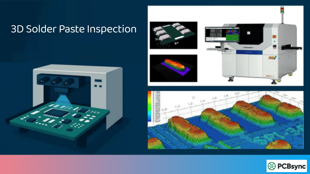
3D Solder Paste Inspection is an automated optical measurement system positioned between the stencil printer and pick-and-place machine in an SMT assembly line. Its job is to verify that every solder paste deposit meets specifications for volume, height, area, and position before components are placed.
Unlike manual visual inspection or basic 2D camera systems, 3D SPI creates a complete topographical map of each paste deposit. It uses structured light projection or laser triangulation to measure the actual three-dimensional shape of the solder paste, not just its footprint.
The technology matters because solder paste is inherently a three-dimensional material. A deposit might look perfectly fine from above (good area coverage, centered on the pad), but have insufficient height due to stencil clogging or paste degradation. That reduced volume leads directly to weak or open solder joints after reflow.
Why 3D SPI Replaced 2D Inspection Systems
Early solder paste inspection relied on 2D grayscale imaging. These systems could detect missing paste, gross bridging, and severe misalignment. However, they had a fundamental limitation: they couldn’t measure paste height or volume.
Consider two identical-looking deposits from above. Both cover the same pad area. Both appear centered. But one has a height of 150 µm (correct) while the other sits at 80 µm (insufficient). The 2D system passes both. The 3D system catches the low volume before it becomes a cold joint or open circuit at final test.
Feature
2D SPI
3D SPI
Area measurement
Yes
Yes
Position/offset detection
Yes
Yes
Height measurement
No
Yes
Volume calculation
No
Yes
Bridge detection
Basic
Advanced
Shape analysis
No
Yes
Repeatability
±10-15%
±2-5%
Fine-pitch capability
Limited
Excellent
The transition from 2D to 3D SPI accelerated as component packages shrank. When you’re placing 0402s and 0201s with pad sizes under 0.5mm, the margin for paste volume error is essentially zero. Modern BGAs with 0.4mm pitch or fine-pitch QFPs absolutely require true 3D measurement for reliable production.
How 3D Solder Paste Inspection Technology Works
Understanding how 3D SPI actually measures paste deposits helps you interpret the data correctly and troubleshoot issues when they arise. Most production systems use one of two primary measurement technologies.
Laser Triangulation Method
A laser line is projected across the PCB surface and paste deposits. A camera mounted at an angle captures the reflected light. Where the laser hits raised paste, the reflected line appears displaced in the camera image. The system calculates height from this displacement using basic triangulation geometry.
Modern laser SPI systems scan the entire board surface by moving the laser/camera head or the PCB itself. Resolution typically reaches 10-15 µm in X/Y and 0.5-1 µm in Z (height). Scan speeds exceed 100 cm²/second on high-end equipment.
Structured Light (Fringe Projection) Method
Instead of a laser line, these systems project a pattern of light and dark stripes onto the surface. The pattern distorts where it hits the three-dimensional paste deposits. By analyzing this distortion with sophisticated algorithms, the system reconstructs a complete 3D surface map.
Structured light offers some advantages for paste inspection. It captures data from a larger field of view simultaneously, reducing scan time. It’s also less affected by the reflective properties of different paste formulations.
Dual and Multi-Projection Systems
One challenge with any single-angle projection system is shadows. A tall paste deposit can block the projected light from reaching adjacent areas. This creates blind spots where the system can’t measure accurately.
High-end 3D SPI systems address this with dual or quad projection heads, illuminating the surface from multiple angles. The software combines data from all projections to eliminate shadow artifacts and provide accurate measurements even on complex topographies like closely-spaced fine-pitch deposits.
Critical Parameters in 3D Solder Paste Inspection
When you’re setting up an SPI program or interpreting inspection results, four parameters matter most. Getting the specifications right for each determines whether your SPI actually catches problems or just generates nuisance alarms.
Solder Paste Volume
Volume is the most critical parameter. It directly predicts whether the resulting solder joint will have adequate material for a reliable connection. Too little volume means weak joints, poor wetting, or opens. Too much means bridging risk or solder balls.
3D SPI calculates volume by integrating the measured 3D profile across the entire deposit area. Results appear in cubic micrometers (µm³) or as a percentage of the theoretical volume (stencil aperture area × stencil thickness).
Typical volume specifications:
Standard components: 80-120% of theoretical
Fine-pitch (≤0.5mm): 90-110% of theoretical
0201/01005 passives: 85-115% of theoretical
BGA pads: 75-125% of theoretical
Volume tolerances tighten considerably for miniature components. A 0201 capacitor might have a theoretical paste volume of only 0.08 mm³. Even a 20% deviation becomes significant at that scale.
Solder Paste Height
Height measurement verifies stencil performance and paste release. Consistent height across the board indicates good snap-off, proper squeegee pressure, and clean apertures. Variation in height points to process issues.
Most stencils run 100-150 µm thick for standard surface mount. Step-down areas for fine-pitch might use 75-100 µm. The SPI height specification typically allows ±15-20% variation from the stencil nominal thickness.
Watch for systematic height variations. If one side of the board consistently runs low, check squeegee wear or parallelism. If height drops through a production run, paste viscosity may be changing due to temperature or working life.
Solder Paste Area
Area measurements verify that paste covers the intended pad surface adequately. Low area coverage can indicate under-aperture design, paste scooping during snap-off, or blocked apertures.
Area specifications typically require:
Minimum 70-80% pad coverage for standard SMD
Minimum 85% for fine-pitch components
Maximum 100-110% (to catch paste spread beyond pad edges)
Area alone doesn’t guarantee a good joint (you need adequate height too), but it catches certain failure modes that volume alone might miss, particularly asymmetric deposits that could cause tombstoning.
Position and Offset
Offset measurement checks that the paste deposit is centered on the pad. Misalignment has several possible causes: stencil stretch, printer alignment drift, PCB fiducial recognition errors, or board dimensional variation.
IPC-7527 guidance on offset:
01005/0201 components: ≤30% of pad dimension
Other SMD: ≤35% of pad dimension
Fine-pitch QFP/BGA: ≤25% of pad dimension
Offset becomes more critical as components shrink. A 50 µm offset that’s barely noticeable on a 1206 pad represents 25% of a 0201 pad width. That’s enough to cause consistent tombstoning.
Understanding the defects that 3D SPI catches helps you correlate inspection results with root causes. Here are the primary failure modes and what they typically indicate about your process.
This is the most common defect and the leading cause of weak or open joints post-reflow. When volume runs low, the resulting solder joint lacks sufficient material to form proper fillets and make reliable electrical contact.
Root causes include:
Aperture clogging from dried paste
Inadequate squeegee pressure
Excessive print speed
Paste viscosity too high
Poor gasket seal between stencil and PCB
Solder Paste Bridging
Bridges occur when paste from adjacent deposits connects, creating potential short circuits after reflow. Fine-pitch components (0.4-0.5mm pitch) are particularly susceptible.
3D SPI detects bridges by analyzing the topography between adjacent pads. Even if the individual deposit volumes are acceptable, a connecting bridge triggers a defect call.
Offset and Registration Defects
Position errors compound through the assembly process. A paste deposit that’s offset 50 µm from pad center, combined with placement tolerance of ±30 µm in the same direction, puts the component 80 µm off-center. That’s enough to cause consistent tombstoning on small passives or partial wetting on fine-pitch leads.
Integrating 3D SPI with SMT Line Process Control
The real power of 3D SPI emerges when you connect it to the rest of your SMT line. Modern systems don’t just inspect—they actively control the process through closed-loop feedback.
Closed-Loop Feedback to Stencil Printer
When SPI detects systematic offset (consistent X, Y, or theta error across multiple boards), it automatically feeds correction values back to the stencil printer. The printer adjusts its alignment for subsequent prints without operator intervention.
This closed-loop control typically maintains print registration within ±15 µm even as stencils stretch with temperature changes or boards vary slightly in dimension. Without it, operators must periodically check alignment and make manual corrections.
Closed Forward Loop to Pick-and-Place
Some advanced systems send paste position data forward to the placement machine. If paste is consistently offset in one direction on a particular pad, the placer can adjust component placement to match, centering the component on the actual paste rather than the theoretical pad location.
This compensation helps prevent tombstoning on small passives where paste offset and placement variation can compound.
Statistical Process Control Integration
3D SPI generates massive amounts of measurement data. Proper SPC integration tracks:
Volume trends over time (detecting paste degradation)
When Cpk values start dropping or control limits get approached, the system alerts operators before defects occur. This predictive capability transforms SPI from defect detection to defect prevention.
3D SPI Equipment Selection Criteria
If you’re evaluating 3D SPI systems for your line, these specifications separate the capable systems from the inadequate ones.
Specification
Minimum Acceptable
High-End Systems
Z-axis resolution
1.0 µm
0.5 µm
Z-axis accuracy
±3 µm
±1 µm
XY resolution
15 µm
10 µm
Measurement repeatability (GR&R)
<10%
<5%
Inspection speed
50 cm²/s
>100 cm²/s
Field of view
20×20 mm
50×50 mm
Minimum pad size
0.15×0.15 mm
0.08×0.08 mm
Measurement Repeatability
GR&R (Gauge Repeatability and Reproducibility) tells you how much variation comes from the measurement system itself versus actual process variation. For SPI to be useful, its measurement variation must be small relative to your process tolerances.
A GR&R under 10% is generally acceptable. Under 5% is excellent. If your SPI system has 15% GR&R, you’ll see excessive false calls and miss real defects because the measurement noise obscures actual problems.
Inspection Speed vs. Accuracy Trade-off
Faster systems use larger fields of view and faster scan rates, but may sacrifice some resolution. Your board complexity determines the right balance. Dense boards with 0201s and fine-pitch components need higher resolution even if it means slower inspection. Simpler boards with larger components can use faster, lower-resolution modes.
Software Capabilities
The hardware captures data, but software determines whether you can use it effectively. Essential software features include:
Gerber/ODB++ import for automatic program generation
Statistical process control with trend analysis
Closed-loop interfaces to printers and placers
Clear defect classification and imaging
Easy tolerance adjustment per component type
IPC Standards for 3D Solder Paste Inspection
Several IPC standards apply to solder paste inspection. Familiarizing yourself with these helps you set appropriate specifications and communicate with customers about quality requirements.
IPC-7527: Requirements for Solder Paste Printing establishes acceptance criteria for solder paste deposits, defining what constitutes acceptable versus defective prints. It provides visual references and measurement guidelines that inform SPI program setup.
IPC-A-610: Acceptability of Electronic Assemblies covers the completed assembly but includes criteria that trace back to paste printing. Understanding these requirements helps you set SPI limits that prevent downstream acceptance issues.
IPC-7525: Stencil Design Guidelines addresses stencil aperture design, including area ratios and aperture shapes that affect paste release. If your SPI consistently flags certain pad types, reviewing stencil design against IPC-7525 often reveals the root cause.
Best Practices for 3D Solder Paste Inspection Implementation
Based on implementing SPI across multiple high-volume lines, these practices consistently improve results:
Calibrate regularly. Most systems need weekly calibration checks and monthly full calibrations. Use the manufacturer’s calibration standard and don’t skip this step. Drift in calibration directly causes false calls and escapes.
Start with conservative tolerances, then optimize. It’s better to begin with tight limits that generate some false calls than loose limits that allow defects. Review escapes after initial production runs and adjust systematically.
Correlate SPI results with post-reflow defects. When AOI or ICT catches a defect, trace it back to the SPI data. Was the paste deposit marginal? Should the SPI limits be tightened for that pad type? This feedback loop continuously improves your detection capability.
Monitor underside stencil cleanliness. Many paste printing defects relate to contamination on the stencil bottom. If SPI flags increasing smearing or bridging, trigger an automatic stencil wipe before problems escalate.
Don’t ignore borderline data. Deposits that consistently test at 85% of volume spec might pass, but they indicate a process drifting toward failure. Investigate before they cross the limit.
ROI and Economic Justification for 3D SPI
3D SPI systems typically cost between $50,000 and $150,000 depending on capabilities. Justifying this investment requires quantifying the defect prevention benefit.
Consider a line producing 500 boards per shift with a 2% paste-related defect rate. Post-reflow rework costs approximately $5-15 per defect depending on complexity. That’s $50-150 per shift in rework costs, or roughly $35,000-100,000 annually on a three-shift operation.
3D SPI typically reduces paste-related defects by 80-90% by catching them before reflow when correction is simple (re-print the board). The rework savings alone often justify the equipment within 1-3 years.
Additional ROI factors include:
Reduced scrap from uncatchable post-reflow defects
Lower field failure rates and warranty costs
Faster new product introduction through better process data
Customer qualification requirements (many automotive and aerospace programs mandate SPI)
Future Trends in 3D Solder Paste Inspection Technology
The 3D SPI market continues evolving. Current development trends include:
AI and machine learning integration improves defect classification. Instead of fixed thresholds, AI systems learn from historical data to distinguish real defects from acceptable variation, reducing false call rates while maintaining escape protection.
Faster inspection speeds keep pace with placement machine capabilities. Leading systems now exceed 100 cm²/second without sacrificing resolution, supporting line takt times under 10 seconds for complex boards.
Enhanced connectivity supports Industry 4.0 initiatives. Real-time data sharing across the factory network enables centralized monitoring and cross-line optimization. CFX (Connected Factory Exchange) and HERMES standards facilitate equipment interoperability.
Expanded inspection capabilities beyond solder paste. Some systems now inspect adhesive dispensing, conformal coating, and even bare board features using the same measurement platform.
Frequently Asked Questions About 3D Solder Paste Inspection
What’s the difference between 3D SPI and AOI?
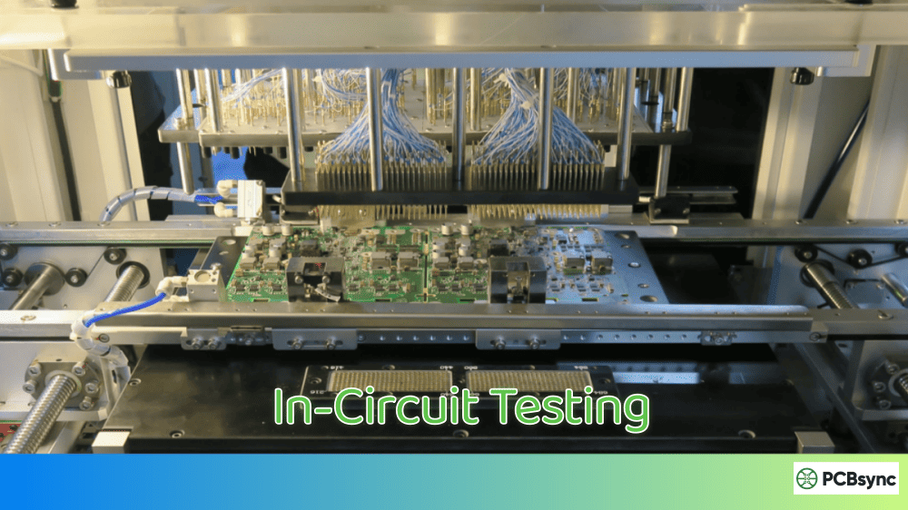
3D SPI inspects solder paste deposits before component placement. AOI (Automated Optical Inspection) examines the assembled board after reflow, checking solder joints, component presence, and orientation. They serve different purposes in the inspection chain—SPI prevents defects, AOI detects them. Most quality-focused lines use both.
How often should I calibrate my 3D SPI system?
Most manufacturers recommend daily verification checks using a standard calibration artifact and full calibration monthly or whenever measurements seem inconsistent. Critical applications (aerospace, medical) may require more frequent calibration with documented records.
Can 3D SPI detect all solder paste defects?
No inspection system catches everything. 3D SPI excels at volume, height, area, and position defects. It’s less effective at detecting some material-related issues like flux separation or oxidized paste that look geometrically correct but won’t reflow properly. Combine SPI with proper paste management and reflow profile control for comprehensive quality.
What causes high false call rates on 3D SPI?
Common causes include: tolerances set too tight for the actual process capability, poor calibration or worn calibration standards, board warpage exceeding the system’s compensation range, reflective surface issues with certain paste types, and software bugs or configuration errors. Systematically eliminate each possibility when false calls become problematic.
Is 3D SPI required for lead-free assembly?
Not technically required, but highly recommended. Lead-free pastes have narrower process windows than tin-lead formulations. The reduced tolerance for volume variation makes 3D SPI effectively necessary for consistent yield with lead-free processes, especially on dense boards with fine-pitch components.
Useful Resources for 3D Solder Paste Inspection
Here are valuable references for deeper study on solder paste inspection:
IPC Standards (Available at ipc.org):
IPC-7527: Requirements for Solder Paste Printing
IPC-7525: Stencil Design Guidelines
IPC-A-610: Acceptability of Electronic Assemblies
Technical Papers:
“The Solder Paste Printing Process: Critical Parameters, Defect Scenarios, Specifications, and Cost Reduction” – Available on ResearchGate
Various application notes from Koh Young, Viscom, CyberOptics, and Mycronic
Industry Publications:
SMT Magazine (iconnect007.com)
Circuits Assembly Magazine (circuitsassembly.com)
SMTnet Forums (smtnet.com) – Active community discussions on SPI topics
3D Solder Paste Inspection has become indispensable for modern electronics manufacturing. With 60-70% of SMT assembly defects originating from the paste printing process, catching these issues before component placement dramatically improves yield, reduces rework costs, and prevents field failures.
The technology has matured significantly. Today’s 3D SPI systems offer sub-micron measurement resolution, closed-loop process control, and sophisticated data analysis. They’re no longer optional equipment for high-reliability applications—they’re table stakes for competitive manufacturing.
If you’re running without 3D SPI, you’re likely shipping defects that could have been caught. If you have 3D SPI but aren’t using closed-loop feedback and SPC analysis, you’re leaving performance on the table. Either way, investing in proper solder paste inspection and using it effectively is one of the highest-return improvements you can make to an SMT line.
The boards know. The data proves it. Measure your paste, control your process, and watch your yield climb.
Inquire: Call 0086-755-23203480, or reach out via the form below/your sales contact to discuss our design, manufacturing, and assembly capabilities.
Quote: Email your PCB files to Sales@pcbsync.com (Preferred for large files) or submit online. We will contact you promptly. Please ensure your email is correct.
Notes: For PCB fabrication, we require PCB design file in Gerber RS-274X format (most preferred), *.PCB/DDB (Protel, inform your program version) format or *.BRD (Eagle) format. For PCB assembly, we require PCB design file in above mentioned format, drilling file and BOM. Click to download BOM template To avoid file missing, please include all files into one folder and compress it into .zip or .rar format.


