Inquire: Call 0086-755-23203480, or reach out via the form below/your sales contact to discuss our design, manufacturing, and assembly capabilities.
Quote: Email your PCB files to Sales@pcbsync.com (Preferred for large files) or submit online. We will contact you promptly. Please ensure your email is correct.
Notes: For PCB fabrication, we require PCB design file in Gerber RS-274X format (most preferred), *.PCB/DDB (Protel, inform your program version) format or *.BRD (Eagle) format. For PCB assembly, we require PCB design file in above mentioned format, drilling file and BOM. Click to download BOM template To avoid file missing, please include all files into one folder and compress it into .zip or .rar format.
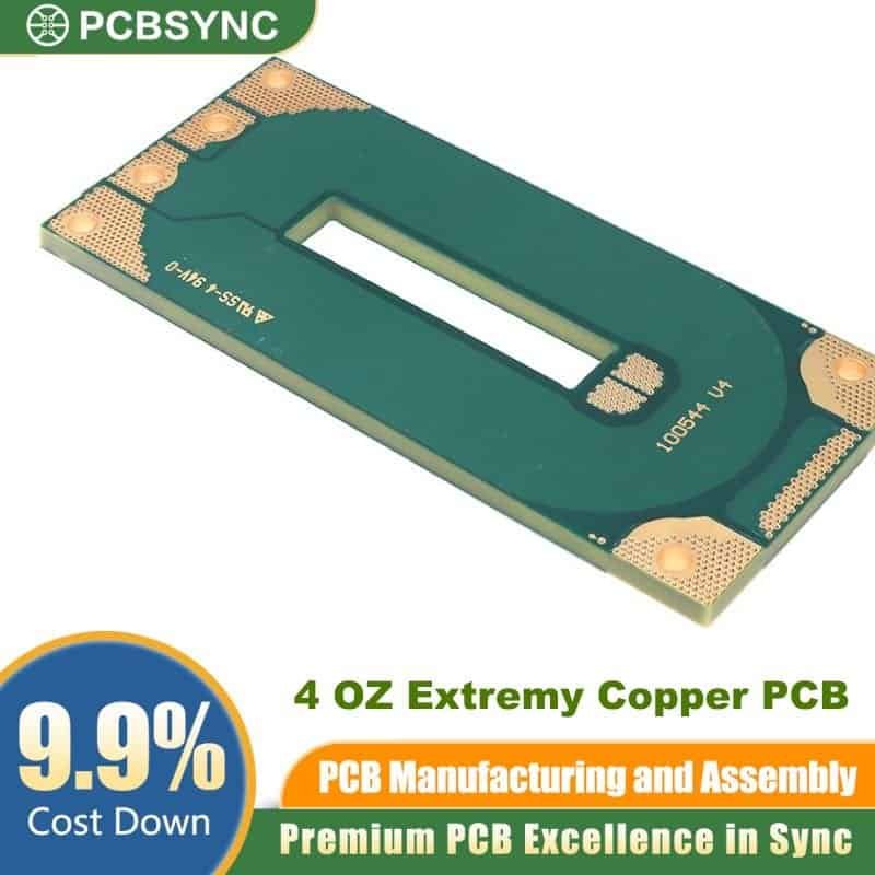
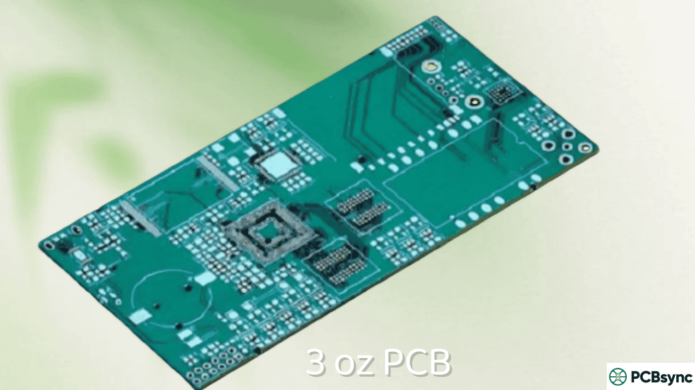
As a PCB engineer who has worked on countless power electronics projects, I can tell you that copper thickness is one of those parameters that can make or break your design. When standard 1 oz copper just isn’t cutting it for your high-current application, 3 oz PCB becomes your go-to solution. In this guide, I’ll walk you through everything you need to know about 3 oz copper PCBs—from understanding the actual thickness measurements to calculating current capacity and nailing the design rules that’ll save you from costly respins.
A 3 oz PCB refers to a printed circuit board where the copper foil thickness equals 3 ounces per square foot on one or more layers. This measurement might sound unusual if you’re used to thinking in millimeters or mils, but it’s actually a holdover from how copper foil manufacturers have historically specified their products.
The “ounce” measurement describes the weight of copper that would cover one square foot of surface area. When 3 ounces of copper is flattened evenly across that square foot, you get a specific thickness that translates to real-world dimensions.
3 oz Copper Thickness Conversion
Copper Weight
Thickness (mils)
Thickness (mm)
Thickness (μm)
0.5 oz
0.7 mils
0.018 mm
17.5 μm
1 oz
1.37 mils
0.035 mm
35 μm
2 oz
2.74 mils
0.070 mm
70 μm
3 oz
4.11 mils
0.105 mm
105 μm
4 oz
5.48 mils
0.140 mm
140 μm
6 oz
8.22 mils
0.210 mm
210 μm
So when we’re talking about a 3 oz PCB, we’re looking at copper that’s roughly 4.1 mils or 105 microns thick—that’s three times thicker than your standard 1 oz copper. This extra thickness translates directly into increased current-carrying capacity and better thermal performance.
Why Heavy Copper Matters: Understanding 3 oz PCB Applications
I’ve seen too many engineers try to squeeze high currents through standard copper boards, only to end up with burnt traces and failed prototypes. A 3 oz PCB becomes necessary when your application falls into one of these categories:
Power Electronics and Energy Systems
The rise of electric vehicles, solar inverters, and high-efficiency power supplies has pushed copper requirements beyond what standard boards can handle. For a 50kW solar inverter, using 3 oz PCB allows you to run wider power buses with better thermal management. We’re seeing over 60% of EVs produced globally now incorporate heavy copper PCBs in their battery management and powertrain systems.
Industrial and Automotive Applications
Motor drives, welding equipment, and automotive control units generate substantial currents that would overwhelm thinner copper. When your motor controller needs to handle 30+ amps continuously, 3 oz PCB gives you the headroom to design reliable traces without making your board look like a copper highway.
Telecommunications and Server Infrastructure
High-speed backplanes in data centers carry significant power alongside their data signals. Using 3 oz PCB for power distribution layers allows engineers to maintain tight tolerances on signal layers while ensuring stable power delivery.
Common Applications for 3 oz PCB
Industry
Application
Typical Current Range
Automotive
EV Battery Management Systems
15-50A
Renewable Energy
Solar Inverters
20-100A
Industrial
Motor Controllers
10-40A
Power Electronics
DC-DC Converters
5-30A
Telecommunications
Server Power Supplies
10-50A
Medical
MRI Equipment Power Systems
15-60A
Defense
Radar Power Modules
20-80A
3 oz PCB Current Capacity: The Numbers That Matter
Here’s where things get practical. Understanding the current-carrying capacity of 3 oz PCB traces is essential for any serious power design. The IPC-2221 and IPC-2152 standards provide the formulas and charts we use to calculate this, but let me break down the key relationships.
How Current Capacity Scales with Copper Thickness
The relationship between copper thickness and current capacity isn’t linear—it follows the square root of the cross-sectional area. When you triple the copper thickness (going from 1 oz to 3 oz), you don’t simply triple the current capacity. However, you do get significant improvements.
For a 3 oz PCB, a 10mil-wide external trace can typically handle around 3-4 amps with a 10°C temperature rise, compared to only about 1 amp for the same width in 1 oz copper. That’s roughly a 3x improvement—matching what you’d expect from tripling the cross-sectional area.
3 oz PCB Trace Width vs. Current Capacity Table
The following table shows approximate current capacity for 3 oz PCB external traces with different widths at 10°C and 20°C temperature rise:
Trace Width (mils)
Trace Width (mm)
Current @ 10°C Rise
Current @ 20°C Rise
10
0.254
3.2A
4.5A
20
0.508
5.5A
7.5A
50
1.27
10A
14A
100
2.54
16A
22A
150
3.81
21A
29A
200
5.08
26A
35A
250
6.35
30A
41A
Note: These values are for external (outer layer) traces. Internal layer traces typically carry 30-50% less current due to reduced heat dissipation capability.
Internal vs. External Layer Considerations
One thing that catches a lot of designers off guard is the difference between internal and external layers. On a 3 oz PCB, your external traces can dissipate heat through convection to ambient air, but internal traces are essentially sandwiched between insulating FR-4 material.
The practical implication? If you’re running high currents on internal layers, you’ll need wider traces or you’ll need to derate your current expectations by about 30-50%. This is where having thermal vias connected to copper pours becomes essential for pulling heat away from buried power traces.
3 oz PCB Design Rules and Guidelines
Getting your 3 oz PCB design right the first time requires following some specific rules that differ from standard copper boards. After working through dozens of heavy copper designs, here are the guidelines I’ve found to be critical.
Minimum Trace Width and Spacing
The etching process for heavy copper creates what we call “trapezoidal traces”—the acid undercuts the copper as it etches down, resulting in traces that are narrower at the bottom than at the top. This means you need wider minimum spacing than you’d use with thinner copper.
Copper Weight
Minimum Trace Width
Minimum Spacing
1 oz
3-4 mils
3-4 mils
2 oz
5-6 mils
5-6 mils
3 oz
8-10 mils
8-10 mils
4 oz
10-12 mils
10-12 mils
6 oz
14-16 mils
14-16 mils
For 3 oz PCB designs, I typically set my design rules to 10 mil minimum trace width and 10 mil minimum spacing. Yes, this limits your routing density, but trying to push finer geometries will result in PCB manufacturing issues and potentially shorted traces.
Via Design for 3 oz PCB
Vias in heavy copper boards need special attention. The plated through-hole copper in a 3 oz PCB must be thick enough to handle the current you’re routing through it. Standard via plating adds about 0.5-1 oz of copper to the barrel, which may not be enough for high-current applications.
Via design recommendations for 3 oz PCB:
Use larger via sizes (minimum 12-15 mil drill) for power connections
Increase via pad sizes to at least 25-30 mils diameter
Consider via stitching—multiple smaller vias in parallel rather than single large vias
Specify minimum 1 oz plating in the via barrel for current-carrying applications
Add thermal relief where appropriate, but remove for high-current power connections
Annular Ring Requirements
The annular ring—the copper remaining around a drilled hole—becomes more critical with heavy copper. For 3 oz PCB, you need larger annular rings to ensure manufacturability and reliability.
A good rule of thumb: maintain at least 8 mil annular ring for 3 oz PCB vias. This accounts for drill tolerance and registration errors while ensuring adequate copper connection to the plated barrel.
Solder Mask Considerations
Heavy copper creates significant surface topology that can cause solder mask issues. The thick traces create “cliffs” that the liquid solder mask has difficulty flowing over evenly. On a 3 oz PCB, you may see:
Thin or missing solder mask at trace edges
Pooling of solder mask in low areas between traces
Multiple solder mask coats required for proper coverage
Work with your fabricator to ensure they understand the copper weight and can adjust their solder mask process accordingly. Some manufacturers use curtain coating or multiple screen prints to achieve proper coverage on 3 oz PCB.
Let me be straight with you: 3 oz PCB is more expensive and more challenging to manufacture than standard copper boards. Understanding why helps you make better design decisions and have more productive conversations with your fab house.
Etching Challenges
Standard etching processes optimized for 1 oz copper will over-etch 3 oz PCB features if not adjusted. The longer etch time required for thick copper means:
More lateral etching (undercutting)
Etch compensation needed in CAM (your 10 mil trace might start as 14 mil in the artwork)
Longer processing time per panel
Higher chemical consumption
Layer Registration
Multilayer 3 oz PCB can experience registration challenges during lamination. The thick copper on inner layers creates more potential for movement during the high-temperature lamination process. Using matched copper weights (same thickness on opposite layers) helps prevent warping.
Cost Factors
Expect to pay 20-40% more for a 3 oz PCB compared to equivalent 1 oz construction. The cost drivers include:
More expensive raw material (heavier copper-clad laminate)
Longer etching cycles
More complex process controls
Higher reject rates
Additional solder mask processing
That said, the performance benefits for power applications typically justify the extra cost. The alternative—using thinner copper with wider traces—often results in a larger board that costs more anyway.
Thermal Management with 3 oz PCB
One of the most underappreciated benefits of 3 oz PCB is improved thermal performance. Copper is an excellent thermal conductor (about 400 W/m·K), and tripling its thickness dramatically improves heat spreading and dissipation.
Heat Dissipation Benefits
The thick copper in a 3 oz PCB acts as an integrated heat spreader. For hot components like MOSFETs, IGBTs, or high-power LEDs, placing them on thick copper planes helps:
Reduce junction temperature by improving heat spreading
Even out thermal gradients across the board
Reduce or eliminate the need for external heat sinks
Improve long-term reliability through lower operating temperatures
Calculating Thermal Improvements
Thermal resistance scales inversely with copper thickness. A 3 oz PCB copper plane will have roughly 1/3 the thermal resistance of equivalent 1 oz copper, assuming the same surface area. In practice, I’ve seen thermal resistance reductions of 30-40% when upgrading from standard to heavy copper.
Thermal Via Strategies
For maximum thermal performance with 3 oz PCB, combine thick copper with strategic thermal vias:
Place thermal vias directly under hot components
Use via arrays with 1mm pitch
Fill vias with copper or conductive epoxy for best thermal transfer
Connect vias to copper planes on internal and bottom layers
3 oz PCB Electrical Properties
Beyond current capacity, 3 oz PCB affects other electrical parameters that matter for your design.
Resistance Reduction
Trace resistance scales inversely with cross-sectional area. For 3 oz PCB, you get roughly 1/3 the resistance compared to 1 oz copper for the same trace geometry. The formula is straightforward:
R = ρ × L / (W × T)
Where ρ is copper resistivity (1.72 × 10⁻⁸ Ω·m), L is length, W is width, and T is thickness.
For a 100mm long, 1mm wide trace in 3 oz PCB:
Resistance ≈ 1.6 mΩ (compared to ~4.9 mΩ for 1 oz copper)
This lower resistance translates to:
Reduced I²R power losses
Lower voltage drops across power distribution
Improved efficiency in power conversion circuits
Impedance Considerations
For controlled impedance applications on 3 oz PCB, the increased trace thickness affects impedance calculations. Thicker copper requires narrower traces to achieve the same impedance target, or you’ll need to adjust dielectric spacing.
Work with your fabricator’s impedance calculator or use simulation tools to determine correct dimensions for impedance-controlled 3 oz PCB stackups.
Comparing 3 oz PCB to Other Copper Weights
Choosing the right copper weight depends on your application requirements. Here’s how 3 oz PCB stacks up against alternatives:
Parameter
1 oz PCB
2 oz PCB
3 oz PCB
4 oz+ PCB
Typical Applications
Consumer electronics, signal routing
General power, moderate current
Power electronics, motor drives
Extreme power, busbars
Min Trace/Space
3-4 mils
5-6 mils
8-10 mils
10-14 mils
Relative Cost
Baseline
+10-15%
+20-40%
+50-100%
Current Capacity
Low
Moderate
High
Very High
Thermal Performance
Standard
Good
Excellent
Superior
Manufacturing Complexity
Standard
Moderate
Elevated
Specialized
For most power electronics applications in the 10-50A range, 3 oz PCB hits the sweet spot between capability and cost. You get substantial improvements over 2 oz copper without the extreme design constraints and costs of 4 oz+ heavy copper.
IPC Standards for 3 oz PCB Design
Proper 3 oz PCB design should reference IPC standards for current capacity calculations and design guidelines:
IPC-2221 (Generic Standard on Printed Board Design)
This foundational standard includes the classic charts for trace current capacity. Section 6.2 provides the formulas:
For external traces: I = 0.048 × ΔT^0.44 × A^0.725
For internal traces: I = 0.024 × ΔT^0.44 × A^0.725
Where I is current in amps, ΔT is temperature rise in °C, and A is cross-sectional area in square mils.
IPC-2152 (Standard for Determining Current Carrying Capacity)
This newer standard provides more detailed and accurate guidelines, accounting for factors like board thickness, plane presence, and conductor height. For critical 3 oz PCB power designs, IPC-2152 gives more reliable results.
IPC-6012 (Qualification and Performance Specification)
For Class 3 applications (military, aerospace, medical), IPC-6012 specifies requirements for copper thickness tolerance, plating quality, and testing methods relevant to 3 oz PCB.
Useful Resources for 3 oz PCB Design
Here are the tools and references I regularly use for 3 oz PCB projects:
IPC-2221B: Generic Standard on Printed Board Design
IPC-2152: Standard for Determining Current Carrying Capacity in Printed Board Design
IPC-6012: Qualification and Performance Specification for Rigid Printed Boards
Design Software with Built-in Calculators
Altium Designer: Built-in IPC-2221 calculator in Properties panel
Cadence OrCAD/Allegro: PDN analysis tools for power integrity
KiCad: Free and open-source with PCB calculator utility
Frequently Asked Questions About 3 oz PCB
1. What is the actual thickness of 3 oz copper on a PCB?
A 3 oz PCB has copper that is approximately 4.11 mils (0.105mm or 105 microns) thick per layer. This measurement represents the weight of copper (3 ounces) spread across one square foot of surface area. The “oz” measurement has become the standard way PCB manufacturers specify copper thickness, even though it technically describes weight rather than dimension.
2. How much current can a 3 oz PCB trace safely carry?
Current capacity depends on trace width and acceptable temperature rise. For a 100-mil wide external trace on a 3 oz PCB, you can expect approximately 16A with a 10°C temperature rise, or about 22A with 20°C rise. Internal traces carry about 30-50% less due to reduced heat dissipation. Always use IPC-2221 or IPC-2152 calculations to verify capacity for your specific design. For critical applications, add a 20-30% safety margin to your calculations.
3. What are the minimum trace width and spacing rules for 3 oz PCB?
Most PCB manufacturers recommend 8-10 mil minimum trace width and 8-10 mil minimum spacing for 3 oz PCB. This is significantly wider than the 3-4 mil minimums possible with 1 oz copper. The larger minimums account for the etching undercut that occurs when removing thick copper—the etchant removes copper laterally as it etches downward, creating trapezoidal trace profiles.
4. Is 3 oz PCB more expensive than standard copper weight?
Yes, expect to pay approximately 20-40% more for a 3 oz PCB compared to standard 1 oz construction. The increased cost comes from more expensive raw materials, longer etching processing times, additional solder mask coats required for proper coverage, and higher reject rates during manufacturing. However, for power applications requiring this copper weight, the cost is typically justified by improved performance and reliability.
5. When should I choose 3 oz PCB instead of wider traces on 1 oz copper?
Choose 3 oz PCB when board space is constrained, when you need better thermal performance, or when running multiple high-current paths would make routing impractical with wider 1 oz traces. A 3 oz PCB with a 50-mil trace can carry roughly the same current as a 150-mil trace in 1 oz copper. For dense power electronics, this space savings is significant. Additionally, the better thermal conductivity of thick copper provides heat-spreading benefits that you can’t achieve just by widening traces on thinner copper.
Conclusion: Getting Your 3 oz PCB Design Right
Working with 3 oz PCB opens up design possibilities for power electronics that simply aren’t achievable with standard copper weights. The three-fold increase in copper thickness delivers substantial improvements in current capacity, thermal performance, and trace resistance—all critical factors for modern power applications.
The key to successful 3 oz PCB design lies in understanding and working within its constraints. Respect the minimum trace width and spacing rules, account for via current capacity, plan for proper solder mask coverage, and use the IPC standards to calculate your actual current requirements. Don’t guess—run the numbers.
Whether you’re designing an EV motor controller, a solar inverter, or industrial power supply, 3 oz PCB technology gives you the electrical and thermal performance needed for demanding applications. Just remember to work closely with your PCB fabricator early in the design process—they can help you optimize your stackup and design rules for their specific process capabilities.
The investment in heavy copper pays dividends in reliability. When a board has to handle serious power for years without failure, 3 oz PCB provides the margin that separates professional-grade power electronics from designs that end up as field failures.
This guide reflects practical experience from working with heavy copper PCB designs. Manufacturing capabilities vary between fabricators—always verify your specific design rules with your chosen manufacturer before finalizing your layout.
Inquire: Call 0086-755-23203480, or reach out via the form below/your sales contact to discuss our design, manufacturing, and assembly capabilities.
Quote: Email your PCB files to Sales@pcbsync.com (Preferred for large files) or submit online. We will contact you promptly. Please ensure your email is correct.
Notes: For PCB fabrication, we require PCB design file in Gerber RS-274X format (most preferred), *.PCB/DDB (Protel, inform your program version) format or *.BRD (Eagle) format. For PCB assembly, we require PCB design file in above mentioned format, drilling file and BOM. Click to download BOM template To avoid file missing, please include all files into one folder and compress it into .zip or .rar format.


