Inquire: Call 0086-755-23203480, or reach out via the form below/your sales contact to discuss our design, manufacturing, and assembly capabilities.
Quote: Email your PCB files to Sales@pcbsync.com (Preferred for large files) or submit online. We will contact you promptly. Please ensure your email is correct.
Notes: For PCB fabrication, we require PCB design file in Gerber RS-274X format (most preferred), *.PCB/DDB (Protel, inform your program version) format or *.BRD (Eagle) format. For PCB assembly, we require PCB design file in above mentioned format, drilling file and BOM. Click to download BOM template To avoid file missing, please include all files into one folder and compress it into .zip or .rar format.
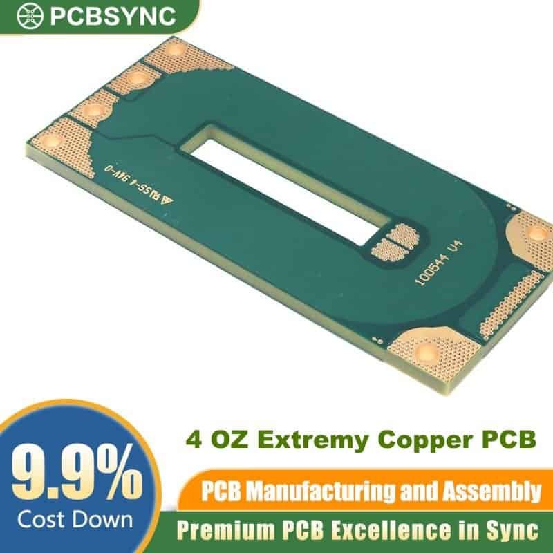
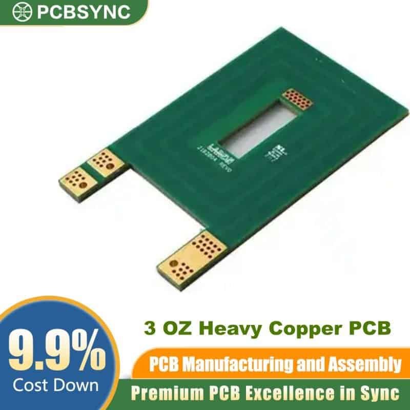
When standard 1oz copper can’t handle your current requirements, 2 oz PCB technology becomes the go-to solution. I’ve designed dozens of power supply boards, motor controllers, and automotive systems where the jump from 1oz to 2oz copper made the difference between a reliable product and a board with burnt traces.
Here’s the quick answer: 2 oz PCB refers to circuit boards with copper weighing two ounces per square foot, producing a thickness of approximately 70 micrometers (2.8 mils). This doubles the copper cross-section compared to standard 1oz boards, enabling roughly twice the current capacity for the same trace width.
This comprehensive guide covers everything engineers need to know about 2oz PCB technology—from precise specifications to practical design guidelines that will help you build reliable high-current circuits.
2 oz PCB describes a printed circuit board manufactured with copper foil weighing two ounces per square foot. When this copper is spread uniformly across that area, it creates a layer approximately 70 micrometers (2.8 mils) thick—exactly double the thickness of standard 1oz copper.
The ounce-based measurement system comes from the copper foil industry, where weighing sheets proved more practical than measuring microscopic thicknesses. Since copper density is constant (8.96 g/cm³), weight directly correlates to thickness, and PCB manufacturers adopted this convention decades ago.
Understanding the 2oz Copper Specification
The math behind the specification:
Two ounces = 56.7 grams
One square foot = 929 square centimeters
Result: 70 micrometers of copper thickness
This thickness provides substantially lower electrical resistance than 1oz copper, directly translating to higher current capacity, reduced voltage drop, and improved thermal performance. For power electronics applications, these benefits often justify the additional cost and pcb manufacturing complexity.
2 oz PCB Thickness Conversion Table
Engineers work across different unit systems depending on their tools and regions. Here’s a complete conversion reference for 2oz PCB copper:
Unit
2oz Copper Value
Notes
Micrometers (μm)
70 μm
Nominal specification
Mils
2.8 mils
Common in US specifications
Millimeters (mm)
0.070 mm
Metric equivalent
Inches
0.0028 inches
Rarely used directly
Microns (actual)
~63-78 μm
Range after processing per IPC
Nominal vs. Finished Thickness
Like all copper specifications, the nominal 2oz value (70 μm) isn’t exactly what ends up on your finished board. According to IPC-4562A and IPC-6012:
For inner layers: 2oz copper typically measures 60-70 μm after fabrication, accounting for surface preparation and micro-etching processes.
For outer layers: Plating adds copper, often resulting in 78-85 μm finished thickness. IPC-6012 Class 2 specifies minimum finished thickness of 78.7 μm for 2oz outer layers after plating.
Understanding these variations matters for impedance calculations and thermal modeling. Always confirm actual thickness values with your fabricator rather than assuming nominal specifications.
The decision to use 2oz copper isn’t arbitrary—it addresses specific engineering challenges that 1oz copper cannot solve efficiently.
Doubled Current Carrying Capacity
The primary driver for 2oz PCB selection is current capacity. With twice the copper cross-section, a 2oz trace can carry approximately twice the current of a 1oz trace at the same width and temperature rise.
For example:
A 100-mil wide trace on 1oz copper: ~3.5A at 10°C rise
The same trace on 2oz copper: ~6-7A at 10°C rise
This doubling effect allows designers to either carry more current with existing trace widths or maintain current levels with narrower traces—valuable for dense layouts.
Reduced Electrical Resistance
Resistance is inversely proportional to conductor cross-sectional area. Doubling copper thickness cuts DC resistance in half:
Trace Width
1oz Resistance
2oz Resistance
Reduction
10 mil
13 mΩ/inch
6.5 mΩ/inch
50%
20 mil
6.5 mΩ/inch
3.25 mΩ/inch
50%
50 mil
2.6 mΩ/inch
1.3 mΩ/inch
50%
100 mil
1.3 mΩ/inch
0.65 mΩ/inch
50%
Lower resistance means less voltage drop across power distribution traces—critical in applications with tight voltage regulation requirements.
Improved Thermal Performance
Copper’s excellent thermal conductivity (400 W/m·K) makes it an effective heat spreader. Thicker copper conducts heat more effectively away from hot components:
Heat spreading: 2oz copper planes spread heat over larger areas, reducing hot spots
Thermal vias: 2oz PTH barrels conduct more heat to inner layers
Component cooling: Exposed copper pads with 2oz thickness provide better heatsinking
In power electronics where components dissipate significant heat, 2oz copper can reduce operating temperatures by 10-20°C compared to 1oz designs.
Enhanced Mechanical Robustness
The additional copper thickness provides structural benefits:
Stronger PTH barrels: Less susceptible to thermal cycling fatigue
More robust pads: Better withstand component insertion and rework
Reduced flexing: Stiffer boards in larger formats
These mechanical advantages improve long-term reliability, particularly in harsh environments with thermal cycling and vibration.
2 oz PCB Current Carrying Capacity
Understanding current capacity is essential for reliable 2oz PCB designs. The following tables provide detailed guidelines based on IPC-2221 standards.
External Layer Current Capacity (2oz Copper)
External traces dissipate heat more effectively, allowing higher current density:
Trace Width
10°C Rise
20°C Rise
30°C Rise
40°C Rise
5 mil
0.8 A
1.1 A
1.4 A
1.6 A
10 mil
1.5 A
2.1 A
2.6 A
3.0 A
20 mil
2.6 A
3.6 A
4.5 A
5.2 A
30 mil
3.5 A
4.9 A
6.0 A
6.9 A
50 mil
5.2 A
7.2 A
8.8 A
10.2 A
75 mil
7.0 A
9.8 A
12.0 A
13.8 A
100 mil
8.5 A
11.8 A
14.5 A
16.7 A
150 mil
11.5 A
16.0 A
19.6 A
22.6 A
200 mil
14.0 A
19.5 A
24.0 A
27.6 A
Internal Layer Current Capacity (2oz Copper)
Internal traces have reduced heat dissipation—approximately 50% of external layer capacity:
Trace Width
10°C Rise
20°C Rise
30°C Rise
40°C Rise
5 mil
0.4 A
0.55 A
0.7 A
0.8 A
10 mil
0.75 A
1.05 A
1.3 A
1.5 A
20 mil
1.3 A
1.8 A
2.25 A
2.6 A
30 mil
1.75 A
2.45 A
3.0 A
3.45 A
50 mil
2.6 A
3.6 A
4.4 A
5.1 A
75 mil
3.5 A
4.9 A
6.0 A
6.9 A
100 mil
4.25 A
5.9 A
7.25 A
8.35 A
150 mil
5.75 A
8.0 A
9.8 A
11.3 A
200 mil
7.0 A
9.75 A
12.0 A
13.8 A
Factors Affecting Real-World Current Capacity
These table values assume isolated traces. Real-world capacity depends on additional factors:
Nearby copper: Adjacent traces and planes provide heat sinking that can increase effective current capacity by 20-50%.
Thermal vias: Via arrays connecting to internal planes significantly improve heat dissipation, potentially doubling the basic current rating.
Ambient temperature: Higher ambient reduces allowable current. Derate by approximately 2.5% per 10°C above 25°C ambient.
Duty cycle: Pulsed currents allow higher peak values. For 50% duty cycle, multiply table values by approximately 1.4.
Altitude: Reduced air density at high altitude impairs convective cooling. Derate by 1% per 1000 feet above 5000 feet.
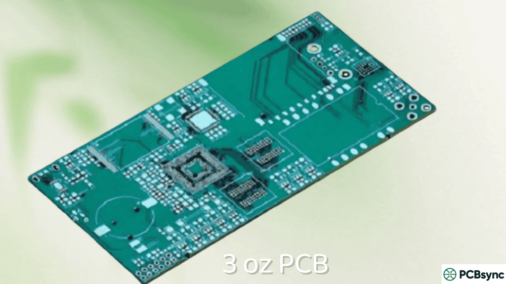
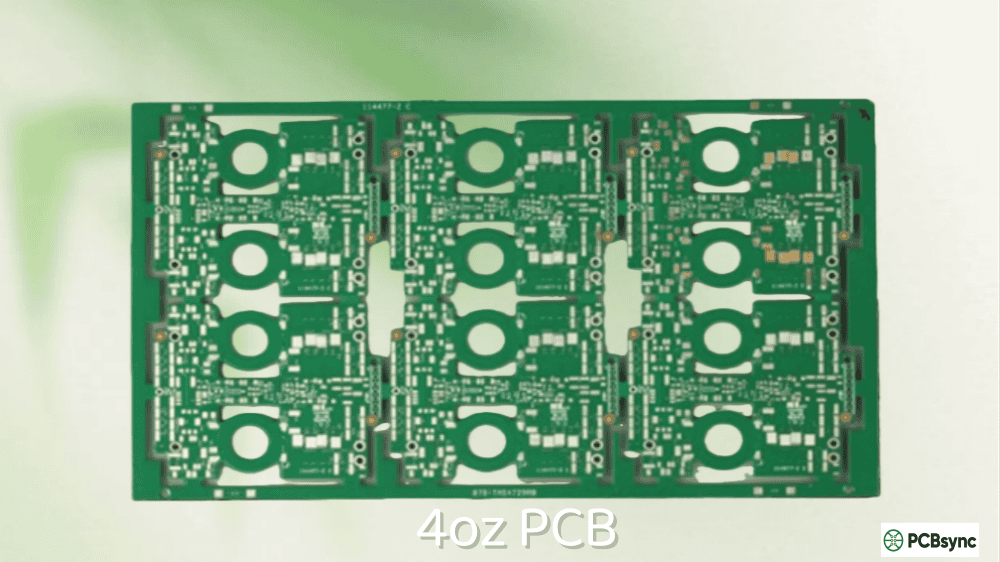
2 oz PCB vs Other Copper Weights
Choosing the right copper weight requires understanding how 2oz compares to alternatives:
Parameter
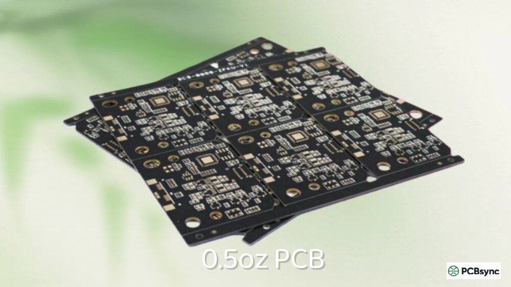
0.5 oz
1 oz
2 oz
3 oz
Thickness (μm)
17-18
34-35
68-70
102-105
Thickness (mils)
0.7
1.37
2.8
4.2
Sheet Resistance (mΩ/sq)
1.0
0.5
0.25
0.17
Min Trace Width
3 mil
4 mil
5 mil
6-8 mil
Min Spacing
3 mil
4 mil
5 mil
8-10 mil
Current (20mil, 10°C rise, ext)
0.9 A
1.7 A
2.6 A
3.3 A
Relative Material Cost
0.9x
1.0x
1.3x
1.6x
Etch Time
Fastest
Standard
2x
3x
Typical Applications
HDI, signals
General
Power, automotive
Heavy copper
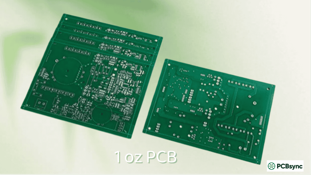
When 1oz Is Sufficient
Standard 1oz copper works well for:
Signal routing with currents under 1A
Digital logic circuits
Low-power analog designs
Cost-sensitive consumer products
Fine-pitch components requiring narrow traces
When 2 oz PCB Is the Right Choice
2 oz PCB becomes necessary when:
Trace currents exceed 1-2A regularly
Power distribution requires minimal voltage drop
Thermal spreading is critical for heat management
Applications demand enhanced reliability margins
Space constraints prevent widening traces sufficiently
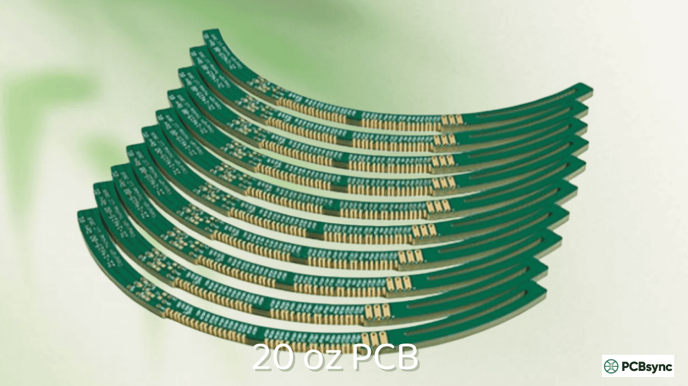
When to Consider 3oz or Heavier
Move beyond 2oz when:
Currents exceed 10A per trace
Designs require extreme thermal conductivity
Military/aerospace specifications mandate heavy copper
Power bus bars need to be integrated into PCB
Applications for 2 oz PCB Technology
The enhanced current capacity and thermal performance of 2oz copper make it essential for specific application categories.
Power Supply and Converter Design
Switch-mode power supplies—whether isolated DC-DC converters, AC-DC power supplies, or point-of-load regulators—benefit significantly from 2oz copper:
High-current output stages: The rectifier and output filter sections often carry 10-50A or more. 2oz copper keeps voltage drops manageable and temperatures under control.
Primary-side switching: Even at lower currents, reduced losses improve efficiency. A 0.5% efficiency improvement in a 500W supply saves 2.5W of heat.
Thermal management: Power semiconductors dump heat into copper planes. 2oz planes spread this heat more effectively, reducing heatsink requirements.
Motor Control and Drives
Variable frequency drives, servo controllers, and brushless DC motor drivers handle substantial currents with high dV/dt transients:
Phase outputs: Motor phase currents of 10-100A require robust copper. 2oz enables reasonable trace widths.
DC bus distribution: The DC link between input rectifier and inverter stage needs low-impedance distribution.
Successfully designing with 2oz copper requires adapting standard PCB design practices to account for thicker copper’s capabilities and limitations.
Trace Width and Spacing Rules
Thicker copper requires larger minimum features due to etching characteristics:
Feature
2oz Capability
Notes
Minimum Trace Width
5 mil (125 μm)
Standard capability
Advanced Trace Width
4 mil (100 μm)
Requires process control
Minimum Spacing
5 mil (125 μm)
Standard capability
Advanced Spacing
4 mil (100 μm)
Higher risk of shorts
Typical Production
6/6 mil
Safe design target
The increased etch time for 2oz copper causes more lateral etching (undercut), which is why minimum features must be larger than with 1oz copper.
Power Distribution Design
Effective power distribution on 2oz PCB involves several strategies:
Solid planes: Where possible, use solid copper planes for power distribution. Even a small 2oz plane offers milliohm-level resistance.
Wide traces: For routed power, use the widest traces your layout allows. More copper is always better for power paths.
Via arrays: Connect power planes using multiple vias in parallel. Calculate via current capacity and ensure adequate via count:
Via Size
2oz Via Current (10°C rise)
8 mil
0.5 A
10 mil
0.7 A
12 mil
0.9 A
15 mil
1.2 A
20 mil
1.8 A
For a 10A connection, you’d need approximately 14 x 10-mil vias or 8 x 15-mil vias.
Copper pours: Fill unused areas with copper pours connected to power or ground. This provides additional current paths and improves thermal performance.
Thermal Management Strategies
2oz copper excels at thermal management when designed correctly:
Thermal relief connections: For hand-soldering, use thermal reliefs on pads connecting to planes. For reflow-only assembly, direct connections provide better thermal performance.
Exposed copper pads: Place exposed copper pads under hot components (power MOSFETs, regulators, power resistors). Connect these to internal planes via thermal via arrays.
Thermal via arrays: Under hot components, place via arrays connecting to inner layer planes. Via pitch of 1mm provides good thermal transfer.
Heat spreading planes: Dedicate inner layers to thermal spreading. Even a partial plane significantly improves heat distribution.
Microstrip: A 50Ω single-ended trace on 2oz copper over 4-mil prepreg (Dk ~4.2) requires approximately 9-10 mils width—wider than 1oz due to thicker copper.
Stripline: Centered 50Ω stripline requires approximately 5-6 mils width with 2oz copper.
Differential pairs: 100Ω differential impedance typically uses 5-6 mil traces with 6-8 mil spacing.
The thicker copper affects impedance calculations significantly. Always verify with your fabricator’s impedance modeling tools—don’t rely on generic calculators without specifying actual copper thickness.
Stack-up Considerations
When designing 2oz PCB stack-ups:
Symmetric copper weights: Maintain symmetric copper weights above and below the board center to prevent warping:
Good (symmetric):
L1: 2 oz
L2: 1 oz
L3: 1 oz
L4: 2 oz
Poor (asymmetric):
L1: 2 oz
L2: 2 oz
L3: 1 oz
L4: 1 oz
Prepreg selection: Thicker copper requires more resin to fill the additional copper relief. Work with your fabricator on appropriate prepreg selection.
Overall thickness: 2oz copper adds significant thickness. A 4-layer board with 2oz on all layers is approximately 0.2mm thicker than the same board with 1oz copper.
Manufacturing Considerations for 2 oz PCB
Understanding fabrication realities helps you design boards that manufacture reliably.
Etching Challenges
2oz copper requires approximately twice the etch time of 1oz copper. During this extended etching:
Lateral undercut: The etchant removes copper from trace sidewalls as well as tops. This creates trapezoidal trace cross-sections and requires fabricators to compensate feature sizes.
Feature uniformity: Longer etch times increase variation across the panel. Features near panel edges may etch differently than those in the center.
Fine feature limits: The combination of undercut and variation makes features below 5 mils risky on 2oz copper with standard processing.
Plating Considerations
For outer layers, the plating process adds complexity:
Starting copper: Fabricators may start with 1oz base copper and plate up to achieve 2oz finished thickness. This approach improves fine-feature capability but adds processing steps.
Plating uniformity: Electroplating deposits more copper on panel edges and near large copper features. This can cause thickness variation.
Specification clarity: Distinguish between “2oz base copper” and “2oz finished copper” in your fabrication notes to avoid confusion.
Soldermask Challenges
Thicker copper creates deeper “canyons” between traces that soldermask must fill:
Multiple coats: Fabricators may need multiple soldermask applications to adequately cover 2oz topography.
Soldermask dams: Minimum dam widths between pads should be larger—typically 5-6 mils minimum rather than 4 mils.
Exposed copper: Tenting vias becomes more difficult. Consider filled and capped vias for better coverage.
Lead Time and Cost Impact
Expect these differences compared to standard 1oz boards:
Factor
Impact vs. 1oz
Material cost
+20-30%
Processing time
+30-50%
Typical lead time
+2-5 days
Minimum order
May be higher
Yield risk
Slightly higher
For prototypes, these impacts are manageable. For volume production, discuss with multiple fabricators—pricing varies significantly based on their equipment and experience with heavy copper.
Cost Analysis: 2 oz PCB Economics
Understanding the economics helps justify 2oz copper where appropriate.
Direct Cost Factors
Copper foil: 2oz copper foil costs approximately 30% more than 1oz foil per square foot.
Laminate cost: 2oz copper-clad laminates carry premium pricing from material suppliers.
Processing: Extended etch times, potential multiple soldermask coats, and tighter process control add fabrication cost.
Cost Comparison Example
For a typical 4-layer, 100mm x 100mm board:
Configuration
Relative Cost
1oz all layers
1.0x (baseline)
2oz outer / 1oz inner
1.15-1.25x
2oz all layers
1.30-1.45x
3oz outer / 2oz inner
1.50-1.70x
Hidden Cost Savings
While 2oz copper costs more directly, it can reduce system costs:
Fewer layers: Higher current capacity may allow reducing layer count—eliminating two layers often saves more than the copper premium costs.
IPC-2221: Generic Standard on Printed Board Design (current capacity, spacing)
IPC-2152: Standard for Determining Current-Carrying Capacity
IPC-4562A: Metal Foil for Printed Board Applications
IPC-6012: Qualification and Performance Specification for Rigid Printed Boards
IPC-9592: Requirements for Power Conversion Devices
Online Design Calculators
Saturn PCB Design Toolkit: Comprehensive free calculator for trace width, current capacity, via current
Sierra Circuits Trace Width Calculator: Web-based current capacity tool
Advanced Circuits PCB Artist: Design tool with integrated calculators
Altium PDN Analyzer: Power distribution network analysis
Thermal Analysis Tools
ANSYS Icepak: Comprehensive thermal simulation
Mentor FloTHERM: Electronics cooling simulation
Cadence Celsius: Electrothermal co-simulation
Fabricator Resources
Request stack-up files with actual copper thickness values
Use fabricator impedance calculators for accurate modeling
Consult design for manufacturing (DFM) guidelines specific to heavy copper
Frequently Asked Questions About 2 oz PCB
How thick is 2 oz PCB copper in mm and mils?
2 oz PCB copper thickness equals approximately 0.070 mm (70 micrometers) or 2.8 mils nominally. After fabrication processing, actual inner layer thickness typically measures 60-70 μm, while outer layers after plating measure 78-85 μm. These variations matter for impedance calculations and thermal modeling—always confirm actual values with your fabricator rather than assuming nominal specifications.
How much current can 2 oz PCB traces carry?
Current capacity depends on trace width, layer position, and acceptable temperature rise. As guidelines for 10°C rise: a 20-mil wide external trace on 2oz copper carries approximately 2.6A, a 50-mil trace carries about 5.2A, and a 100-mil trace handles around 8.5A. Internal traces have roughly half these capacities due to reduced heat dissipation. For higher temperature rise allowances, capacity increases proportionally—multiply by approximately 1.4 for 20°C rise or 1.7 for 30°C rise.
When should I use 2 oz PCB instead of 1 oz?
Choose 2 oz PCB when your design requires trace currents exceeding 1-2A, needs minimal voltage drop across power distribution, benefits from enhanced thermal spreading for heat management, or demands improved long-term reliability. Common applications include power supplies, motor controllers, automotive electronics, LED drivers, and industrial equipment. If your current requirements can be met with reasonably-sized 1oz traces and thermal management isn’t critical, standard 1oz copper is more cost-effective.
Does 2 oz copper affect PCB impedance?
Yes, copper thickness directly impacts impedance calculations. For 2oz copper, controlled impedance traces require different widths than 1oz designs. A typical 50Ω microstrip on 2oz copper needs approximately 9-10 mils width over standard dielectric—wider than the 7-8 mils required for 1oz copper. Stripline and differential pair dimensions also change. Always use impedance calculators that account for actual copper thickness, and verify calculations with your fabricator’s modeling tools.
What is the cost difference between 1 oz and 2 oz PCB?
2 oz PCB typically costs 25-45% more than equivalent 1oz boards, depending on fabricator, layer count, and quantity. The premium comes from higher copper material costs, extended processing time for etching, and potentially additional soldermask applications. However, this direct cost increase can be offset by system-level savings: reduced layer count due to higher current capacity, smaller heatsinks from better thermal performance, and improved reliability reducing warranty costs. For high-current applications, the premium is usually justified.
Summary: When 2 oz PCB Makes Sense
2 oz PCB technology provides the enhanced current capacity, reduced resistance, and improved thermal performance that power electronics applications demand. At 70 micrometers (2.8 mils) thickness, 2oz copper delivers approximately twice the current-handling capability of standard 1oz boards while significantly improving heat spreading and long-term reliability.
The decision to use 2oz copper should be driven by clear engineering requirements:
Use 2oz PCB when:
Trace currents regularly exceed 1-2A
Power distribution voltage drop is critical
Thermal management challenges exist
Enhanced reliability is required
Space constraints prevent adequate trace widening
Stick with 1oz when:
Current requirements are modest
Standard thermal performance suffices
Fine-pitch routing is required (below 5 mil)
Cost optimization is paramount
Design is predominantly signal routing
For power supply design, motor control, automotive electronics, and industrial applications, 2oz copper has become the expected standard rather than a premium option. The additional material and processing cost is modest compared to the performance and reliability benefits.
When designing your next high-current project, consider 2oz copper early in the design process. The choice affects trace widths, spacing rules, thermal strategy, and stack-up planning. Working with your fabricator to optimize the design for their heavy copper capabilities ensures you get the full benefit of this proven technology.
Inquire: Call 0086-755-23203480, or reach out via the form below/your sales contact to discuss our design, manufacturing, and assembly capabilities.
Quote: Email your PCB files to Sales@pcbsync.com (Preferred for large files) or submit online. We will contact you promptly. Please ensure your email is correct.
Notes: For PCB fabrication, we require PCB design file in Gerber RS-274X format (most preferred), *.PCB/DDB (Protel, inform your program version) format or *.BRD (Eagle) format. For PCB assembly, we require PCB design file in above mentioned format, drilling file and BOM. Click to download BOM template To avoid file missing, please include all files into one folder and compress it into .zip or .rar format.


