Inquire: Call 0086-755-23203480, or reach out via the form below/your sales contact to discuss our design, manufacturing, and assembly capabilities.
Quote: Email your PCB files to Sales@pcbsync.com (Preferred for large files) or submit online. We will contact you promptly. Please ensure your email is correct.
Notes: For PCB fabrication, we require PCB design file in Gerber RS-274X format (most preferred), *.PCB/DDB (Protel, inform your program version) format or *.BRD (Eagle) format. For PCB assembly, we require PCB design file in above mentioned format, drilling file and BOM. Click to download BOM template To avoid file missing, please include all files into one folder and compress it into .zip or .rar format.
As a PCB engineer who’s spent years working with high-power applications, I’ve watched 10 oz PCB technology transform from a niche specialty into a mainstream solution for demanding power electronics. If you’re wrestling with thermal management issues, dealing with current loads that make standard boards sweat, or designing the next generation of EV chargers, this guide will give you everything you need to know about extreme heavy copper design.
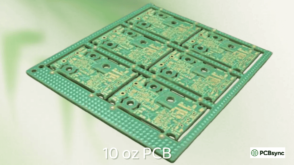
What is a 10 oz PCB?
A 10 oz PCB refers to a printed circuit board with copper layers weighing 10 ounces per square foot. To put that in perspective, most consumer electronics use 1 oz copper, which measures about 35 micrometers (1.37 mils) thick. A 10 oz copper layer measures approximately 350 micrometers (13.8 mils)—that’s nearly ten times thicker than standard boards.
In the industry, we categorize copper thickness as follows:
Category
Copper Weight
Thickness (μm)
Thickness (mils)
Standard Copper
0.5 – 2 oz
17.5 – 70
0.7 – 2.8
Heavy Copper
3 – 6 oz
105 – 210
4.1 – 8.3
Extreme Copper
7 – 10 oz
245 – 350
9.6 – 13.8
Ultra-Heavy Copper
10 – 20 oz
350 – 700
13.8 – 27.6
The 10 oz PCB sits right at the boundary between extreme and ultra-heavy copper territory, making it ideal for applications that need serious current-carrying capacity without going to the absolute extremes of 20 oz designs.
I’ve had countless conversations with engineers who initially thought 2 oz or 3 oz copper would handle their requirements. After thermal testing revealed hot spots and voltage drops, they came back asking about heavier copper options. Here’s why 10 oz PCB makes sense for certain applications.
Superior Current-Carrying Capacity
The relationship between copper thickness and current capacity isn’t linear—it’s governed by thermal dynamics. A 10 oz PCB can handle substantially more current than standard boards while maintaining safe operating temperatures.
Copper Weight
Approximate Current Capacity (per trace)
Typical Applications
1 oz
10 – 30 A
Consumer electronics, signal routing
4 oz
50 – 100 A
Industrial controls, motor drivers
10 oz
100 – 500 A
EV charging, power converters, welding equipment
20 oz
500+ A
Nuclear power systems, heavy industrial
These figures assume appropriate trace widths and acceptable temperature rise. The IPC-2152 standard provides detailed guidelines for calculating exact current capacity based on your specific parameters.
Enhanced Thermal Management
Copper’s thermal conductivity of 401 W/m·K makes it an excellent heat spreader. With 10 oz copper, your PCB essentially becomes an integrated heatsink. I’ve seen designs where switching from 2 oz to 10 oz copper reduced component junction temperatures by 15-20°C—that’s significant when you’re trying to extend MOSFET lifespan.
The thermal benefits include:
30-50% improvement in heat dissipation compared to standard PCBs
40-60% reduction in localized hot spots
Reduced dependency on external heatsinks and cooling fans
More uniform temperature distribution across the board
Mechanical Durability
Thicker copper provides mechanical advantages that often get overlooked. The 10 oz PCB construction offers:
Enhanced resistance to thermal cycling stress
Stronger pad adhesion for heavy components
Better vibration resistance in automotive and aerospace applications
Improved via integrity under high-current conditions
Designing for 10 oz copper requires adjusting your mindset from standard PCB rules. Here’s what I’ve learned from years of heavy copper design work.
Trace Width and Spacing Requirements
Thick copper etches differently than thin copper. The etchant undercuts more aggressively, which affects your minimum feature sizes. Here’s a practical guide:
Copper Weight
Minimum Trace Width
Minimum Spacing
Etch Factor
1 oz
4 mils
4 mils
Low
3 oz
8 mils
8 mils
Medium
6 oz
15-18 mils
15-18 mils
High
10 oz
20-25 mils
20-25 mils
Very High
These are conservative guidelines. Your fabricator may have different capabilities, so always verify before finalizing your design rules.
Via Design for High Current
Standard vias become current bottlenecks in 10 oz PCB designs. A single via rated for 1-2A on a standard board won’t handle the currents you’re dealing with. Instead, use via arrays.
For a 50A current path, I typically specify 20-30 vias distributed across the connection area. Thermal vias under power components need even higher density—30-50 vias per component footprint is common practice for power MOSFETs.
Key via design considerations:
Use larger via diameters (20 mil or greater)
Specify heavier copper plating (1.5-2 mil minimum)
Design via arrays rather than single vias for current transfer
Place thermal vias in dense arrays (20-30 mil pitch) beneath heat-generating components
Thermal Relief and Plane Connections
Direct connection to heavy copper planes makes soldering difficult and can cause cold joints. Always use thermal reliefs, but adjust them for your copper weight:
Standard 1 oz: 4 spokes, 10-12 mil width
10 oz PCB: 4-8 spokes, 25-40 mil width
Balance thermal resistance with current-carrying requirements
Layer Stackup Considerations
When designing multilayer 10 oz PCBs, balance is critical. I recommend mirroring heavy copper layers to prevent board warpage:
Example 6-layer stackup for mixed signal and power:
Layer 1: 10 oz (Power, component side)
Layer 2: 1-2 oz (Control signals)
Layer 3: 2 oz (Ground plane)
Layer 4: 2 oz (Ground plane)
Layer 5: 1-2 oz (Control signals)
Layer 6: 10 oz (Power, bottom side)
This symmetric stackup minimizes bow and twist while providing massive current capacity on the outer layers.
Manufacturing Challenges for 10 oz PCB
Understanding PCB manufacturing challenges helps you design boards that fabricators can actually build. Here’s what makes 10 oz PCB production difficult.
Registration and Layer Alignment
The accumulated tolerance of ultra-thick copper layers can cause layer misalignment. Tight registration requirements become harder to meet as copper thickness increases. Budget for larger annular rings and more generous tolerances than you’d specify for standard boards.
Aspect Ratio Limitations
Drilling through 10 oz copper multiple times in a multilayer stackup creates high aspect ratio holes. Plating these reliably requires specialized equipment and process control. Standard fabricators max out around 8:1 aspect ratio, while 10 oz specialists may handle 14:1 or better.
Surface Finish Consistency
Achieving uniform plating on the rough matte side of heavy copper foil requires precision process control. Hot Air Solder Leveling (HASL) may produce uneven results. Consider ENIG or OSP finishes for better consistency.
Lamination Quality
Bonding layers without voids or resin starvation is challenging with thick copper. The copper acts as a heatsink during lamination, requiring longer press cycles and careful prepreg selection. High Tg materials (170°C or higher) are typically required for reliable 10 oz PCB production.
The investment in 10 oz PCB makes sense when your application truly demands it. Here are the industries driving demand.
Electric Vehicle Charging Infrastructure
EV fast chargers handling 100-350 kW need to convert grid power efficiently. The power conversion stages, battery management systems, and DC-DC converters all benefit from 10 oz copper’s thermal and current-handling capabilities. I’ve worked on 150 kW charger designs where 10 oz copper reduced overall board size by 40% compared to multi-board solutions with standard copper.
Renewable Energy Systems
Solar inverters and wind turbine power converters operate continuously at high power levels. The 10 oz PCB technology supports power densities that would overwhelm standard boards. These applications also benefit from the improved reliability that comes with better thermal management.
Industrial Motor Drives
Variable frequency drives for industrial motors may switch currents of 50-200A at frequencies up to 20 kHz. The combination of high current and fast switching creates severe thermal stress that 10 oz copper handles effectively.
Power Supply Units
Server-grade power supplies targeting 3+ kW output with 95%+ efficiency pack enormous power density into 1U or 2U rack spaces. Heavy copper enables the current densities these designs require.
Medical Equipment
MRI systems, X-ray generators, and other medical imaging equipment require reliable high-power electronics. The enhanced reliability of 10 oz PCB construction meets the stringent requirements of medical applications.
IPC Standards for 10 oz PCB Design
Two IPC standards are essential for heavy copper design work:
IPC-2152: Current Carrying Capacity
This 2009 standard replaced the outdated trace width charts from IPC-2221. IPC-2152 is based on actual thermal testing rather than theoretical calculations, making it significantly more accurate for heavy copper applications. The standard covers copper weights up to 3 oz directly, with guidance for extrapolating to heavier weights.
Key IPC-2152 considerations:
Internal conductors run hotter than external conductors
Board thickness affects conductor temperature
Copper planes near traces provide cooling
Parallel conductors interact thermally
IPC-A-600: Acceptability Criteria
This standard defines visual and dimensional acceptance criteria for finished PCBs. For 10 oz PCB production, pay attention to:
Copper thickness tolerances
Etch factor and trace width accuracy
Via plating thickness requirements
Surface finish uniformity
Cost Considerations for 10 oz PCB Projects
Let’s be realistic about costs. 10 oz PCB fabrication costs 3-5 times more than standard boards of similar complexity. Here’s the breakdown:
Cost Factor
Impact
Mitigation
Material
Higher raw copper cost
Use heavy copper only where needed
Processing
Longer etch and plating cycles
Consolidate heavy copper designs
Tooling
Specialized drill bits, longer tool wear
Plan for larger production runs
Yield
Lower yield due to fabrication challenges
Work with experienced suppliers
Testing
Extended electrical and thermal testing
Budget for comprehensive qualification
To optimize costs, consider hybrid designs that use 10 oz copper only on power layers while standard copper handles signal routing.
Design Software Considerations for 10 oz PCB
Your EDA tool needs proper configuration for heavy copper design. Here’s what I recommend adjusting in your design environment.
Design Rule Settings
Standard design rules won’t work for 10 oz copper. Update your design rules to reflect larger trace widths, increased clearances, and appropriate via sizes. Most EDA tools allow copper-weight-specific rules—take advantage of this feature to enforce heavy copper requirements automatically.
Thermal Simulation
Before committing to fabrication, run thermal simulations with accurate copper thickness settings. Tools like Altium Designer, Cadence Allegro, and Ansys Icepak can model heat distribution through heavy copper layers. Verify that your worst-case current paths stay within acceptable temperature limits.
Impedance Considerations
Thicker copper affects impedance calculations. The increased copper height lowers trace impedance, potentially requiring dielectric thickness adjustments to maintain target values. Work with your stackup vendor to fine-tune impedance control when mixing 10 oz power layers with signal routing layers.
Selecting a 10 oz PCB Manufacturer
Not every PCB shop can produce quality 10 oz boards. Here’s what to look for:
Essential capabilities:
Documented experience with 8-10 oz copper production
Process controls for thick copper etching and plating
High-reliability lamination capabilities
Testing equipment for high-current applications
Questions to ask:
What’s your yield rate on 10 oz production?
Can you provide samples or references from similar projects?
What design support do you offer for heavy copper layouts?
What testing do you perform on heavy copper boards?
Useful Resources for 10 oz PCB Design
These resources have helped me throughout my heavy copper design career:
Standards and Guidelines:
IPC-2152: Current Carrying Capacity Standard (shop.ipc.org)
IPC-2221: Generic Standard on Printed Board Design
Altium Designer with built-in IPC-2152 integration
Technical Documentation:
EPEC Heavy Copper Design Guide (epectec.com/articles)
IPC-2152 presentation materials available through IPC (ipc.org)
Frequently Asked Questions About 10 oz PCB
What is the current capacity of a 10 oz copper trace?
A 10 oz copper trace can carry 100-500A depending on trace width and acceptable temperature rise. For a 10mm wide trace with 20°C temperature rise, expect approximately 150-200A capacity on external layers. Always verify using IPC-2152 calculations for your specific parameters, as internal versus external placement significantly affects capacity.
How much does 10 oz PCB fabrication cost?
10 oz PCB fabrication typically costs 3-5 times more than equivalent standard PCBs. A simple 2-layer 10 oz board might cost $500-1500 for prototype quantities, while complex multilayer designs can exceed $3000-5000 per piece. Volume production reduces per-unit costs significantly, making 10 oz economical for production runs of 100+ boards.
Can any PCB manufacturer produce 10 oz copper boards?
No, 10 oz PCB production requires specialized equipment and expertise that most standard fabricators lack. Look for manufacturers specifically advertising heavy copper capabilities with documented experience at 10 oz weights. Request references and yield data before committing to a production order.
What’s the difference between 10 oz PCB and standard heavy copper PCB?
Standard heavy copper typically refers to 3-4 oz copper weights, which handle moderate high-current applications. 10 oz PCB falls into the extreme copper category, offering substantially higher current capacity and thermal performance. The manufacturing processes are similar but require more precise control and longer processing times for 10 oz production.
How do I calculate trace width for 10 oz copper?
Use the IPC-2152 standard or online calculators that implement these formulas. The key inputs are current requirement, acceptable temperature rise, copper weight, and trace location (internal vs. external layer). For 10 oz copper, expect trace widths to be narrower than equivalent current paths in standard copper, which enables higher power density. Note that standard IPC-2152 charts only extend to 3 oz, so extrapolation is required for 10 oz calculations.
Conclusion
The 10 oz PCB represents the engineering solution for applications where standard copper simply can’t keep up with thermal and electrical demands. From EV charging stations to industrial power converters, this technology enables designs that would be impossible with conventional PCB construction.
Success with 10 oz copper requires understanding the unique design constraints, partnering with capable manufacturers, and applying appropriate standards throughout development. The higher cost and complexity pay dividends in system reliability, reduced cooling requirements, and the ability to pack more power into smaller spaces.
If your next project involves serious current loads or thermal challenges, 10 oz PCB technology deserves serious consideration. Start by consulting with your preferred fabricator early in the design process—their input on capabilities and constraints will save you revision cycles and get you to production faster.
Meta Description Suggestion:
10 oz PCB guide covering extreme heavy copper design for high-power applications. Learn trace width calculations, manufacturing requirements, IPC-2152 standards, and design guidelines from experienced PCB engineers. Includes current capacity tables and practical design rules.
Inquire: Call 0086-755-23203480, or reach out via the form below/your sales contact to discuss our design, manufacturing, and assembly capabilities.
Quote: Email your PCB files to Sales@pcbsync.com (Preferred for large files) or submit online. We will contact you promptly. Please ensure your email is correct.
Notes: For PCB fabrication, we require PCB design file in Gerber RS-274X format (most preferred), *.PCB/DDB (Protel, inform your program version) format or *.BRD (Eagle) format. For PCB assembly, we require PCB design file in above mentioned format, drilling file and BOM. Click to download BOM template To avoid file missing, please include all files into one folder and compress it into .zip or .rar format.


