Inquire: Call 0086-755-23203480, or reach out via the form below/your sales contact to discuss our design, manufacturing, and assembly capabilities.
Quote: Email your PCB files to Sales@pcbsync.com (Preferred for large files) or submit online. We will contact you promptly. Please ensure your email is correct.
Notes: For PCB fabrication, we require PCB design file in Gerber RS-274X format (most preferred), *.PCB/DDB (Protel, inform your program version) format or *.BRD (Eagle) format. For PCB assembly, we require PCB design file in above mentioned format, drilling file and BOM. Click to download BOM template To avoid file missing, please include all files into one folder and compress it into .zip or .rar format.
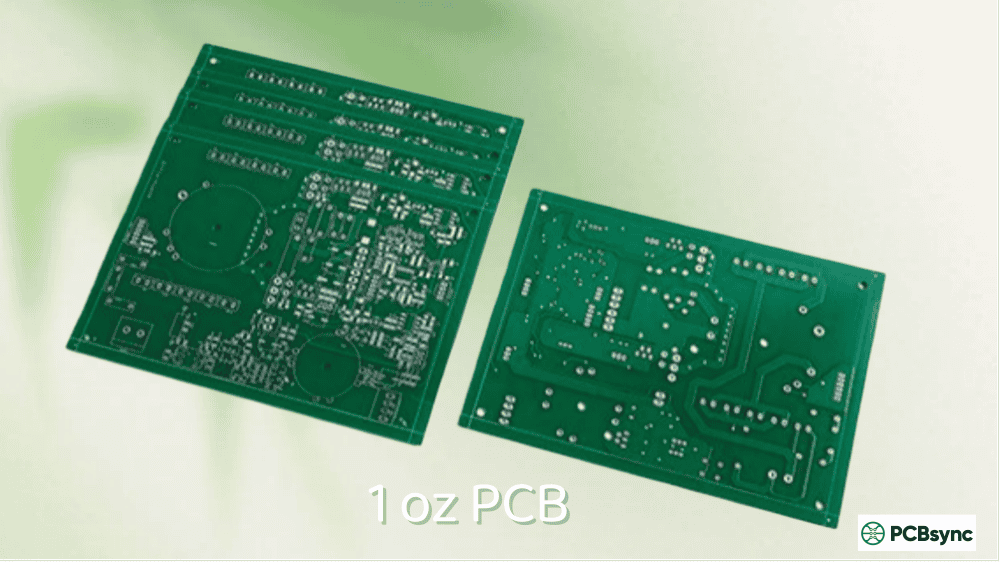
If you’ve worked with printed circuit boards for any length of time, you’ve encountered the term 1oz PCB countless times. It appears in fabricator quotes, stack-up documents, design guidelines, and material specifications. Yet many engineers—even experienced ones—don’t fully understand what this measurement means or why it became the industry standard.
Here’s the quick answer: 1oz PCB refers to circuit boards with copper foil weighing one ounce per square foot, resulting in a thickness of approximately 35 micrometers (1.37 mils). This copper weight has dominated PCB manufacturing for decades because it strikes an ideal balance between electrical performance, manufacturability, and cost.
This guide covers everything you need to know about 1oz PCB technology—from precise thickness conversions to current capacity calculations and practical design guidelines.
1oz PCB describes a printed circuit board manufactured with copper foil weighing one ounce per square foot of area. When copper at this weight is spread uniformly across that surface, it produces a layer approximately 34-35 micrometers thick.
The terminology traces back to the copper foil industry, where weighing sheets proved more practical than measuring their microscopic thickness. Since copper density is constant, weight directly correlates to thickness—and PCB manufacturers adopted this convention decades ago.
The Ounce-to-Thickness Relationship
Understanding the math behind this measurement helps clarify the specification:
One ounce = 28.35 grams
One square foot = 929 square centimeters
Copper density = 8.96 g/cm³
When you spread 28.35 grams of copper evenly across 929 cm², the resulting thickness equals approximately 0.0034 cm or 34 micrometers. This is why “1oz copper” and “35μm copper” are used interchangeably throughout the industry.
1oz PCB Thickness Conversion Table
Engineers work across different unit systems depending on their tools, region, and application. Here’s a comprehensive conversion reference for 1oz PCB copper:
Unit
1oz Copper Value
Notes
Micrometers (μm)
34-35 μm
Nominal specification
Mils
1.37 mils
Common in US specifications
Millimeters (mm)
0.035 mm
Metric equivalent
Inches
0.00137 inches
Rarely used directly
Microns (actual)
~30 μm
After processing per IPC
Nominal vs. Actual Thickness
Here’s something critical that many designers overlook: the nominal 1oz specification (35 μm) isn’t exactly what ends up on your finished board.
According to IPC-4562A and IPC-6012, manufacturing tolerances and processing steps affect final copper thickness. The copper foil itself has a ±10% tolerance from the supplier. Then, fabrication processes like surface preparation and etching can reduce thickness further.
For inner layers, 1oz copper typically measures around 30 μm (1.2 mils) after processing. For outer layers, plating adds copper back, often resulting in 35-45 μm finished thickness depending on the plating specification.
This matters significantly for impedance calculations. If your EDA tool assumes 35 μm but actual thickness is 30 μm on inner layers, your controlled impedance traces will deviate from target values.
The dominance of 1oz copper in PCB manufacturing didn’t happen by accident. Several factors combined to establish this weight as the default specification.
Electrical Performance Balance
1oz copper provides sufficient conductivity for the vast majority of electronic applications. A 10-mil wide trace on 1oz copper can safely carry approximately 1 amp with a 10°C temperature rise—adequate for most signal and moderate power distribution needs.
The sheet resistance of 1oz copper (approximately 0.5 mΩ/square) keeps voltage drops manageable across typical board dimensions while maintaining reasonable trace widths.
Manufacturing Sweet Spot
From a fabrication perspective, 1oz copper hits the manufacturability sweet spot:
Etching: Standard etching processes handle 1oz copper efficiently. Thicker copper requires longer etch times with more undercut, while thinner copper risks over-etching.
Photolithography: Common dry film and liquid photoresists cover 1oz copper adequately. Heavier copper often requires screen-printed resists.
Soldermask: Standard liquid photoimageable (LPI) soldermask at 25-75 μm thickness provides proper coverage over 1oz copper features.
Plating: Electroless and electrolytic plating processes are optimized for building up from 1oz base copper.
Cost Effectiveness
1oz copper foil is widely available from multiple suppliers at competitive prices. It’s stocked by virtually every laminate manufacturer and PCB fabricator worldwide. Specifying anything other than 1oz often triggers longer lead times and higher costs.
Historical Momentum
Once 1oz became established as the default, the entire supply chain optimized around it. Material suppliers stock 1oz laminates. Fabricators calibrate processes for 1oz etching. Design tools default to 1oz assumptions. This infrastructure investment reinforces the standard’s dominance.
1oz PCB Current Carrying Capacity
Understanding how much current your traces can safely carry is essential for reliable 1oz PCB designs. Current capacity depends on trace width, layer position, and acceptable temperature rise.
External Layer Current Capacity
External (outer) layer traces dissipate heat more effectively than buried traces, allowing higher current density:
Trace Width
10°C Rise
20°C Rise
30°C Rise
5 mil
0.5 A
0.7 A
0.9 A
10 mil
1.0 A
1.4 A
1.7 A
20 mil
1.7 A
2.4 A
3.0 A
50 mil
3.2 A
4.5 A
5.5 A
100 mil
5.5 A
7.5 A
9.0 A
Internal Layer Current Capacity
Internal traces have significantly reduced current capacity—approximately 50% of external traces—due to limited heat dissipation:
Trace Width
10°C Rise
20°C Rise
30°C Rise
5 mil
0.25 A
0.35 A
0.45 A
10 mil
0.5 A
0.7 A
0.85 A
20 mil
0.85 A
1.2 A
1.5 A
50 mil
1.6 A
2.2 A
2.8 A
100 mil
2.8 A
3.8 A
4.5 A
These values derive from IPC-2221 guidelines. For critical applications, use IPC-2152 methods or thermal simulation for more accurate analysis.
Factors Beyond Simple Calculations
Real-world current capacity depends on additional factors that simple tables don’t capture:
Nearby copper: Adjacent traces and planes provide heat sinking that increases effective current capacity.
Board thickness: Thicker boards conduct heat to planes and mounting surfaces more effectively.
Ambient temperature: Higher ambient reduces the allowable current for a given temperature rise limit.
Duty cycle: Pulsed currents may allow higher peak values than continuous DC.
Via connections: Vias add thermal mass and can improve or impair current handling depending on configuration.
1oz PCB vs Other Copper Weights
Choosing the right copper weight requires understanding how 1oz compares to alternatives:
Parameter
0.5 oz
1 oz
2 oz
3 oz
Thickness (μm)
17-18
34-35
68-70
102-105
Thickness (mils)
0.7
1.37
2.8
4.2
Sheet Resistance
1.0 mΩ/sq
0.5 mΩ/sq
0.25 mΩ/sq
0.17 mΩ/sq
Min Trace Width
3 mil
4 mil
5 mil
6 mil
Min Spacing
3 mil
4 mil
5 mil
8 mil
Current (10mil, 10°C)
0.55 A
1.0 A
1.5 A
1.9 A
Relative Cost
0.9x
1.0x
1.3x
1.6x
Flex Life
Best
Good
Fair
Poor
When to Choose 0.5 oz Over 1oz PCB
Half-ounce copper makes sense when:
Fine-pitch routing requires traces below 4 mils
Flex circuits need maximum bend life
Inner layers carry only signals (not power)
Cost optimization on high-volume products
When to Choose 2 oz Over 1oz PCB
Two-ounce copper is appropriate when:
Power distribution requires lower resistance
Current levels exceed 1oz capacity at acceptable trace widths
Thermal spreading is needed for heat management
High-reliability applications demand extra margin
When 1oz PCB Is the Right Choice
For most applications, 1oz PCB provides the optimal balance:
Successfully designing with 1oz copper requires understanding its capabilities and working within proven guidelines.
Trace Width and Spacing
Standard 1oz PCB fabrication supports these minimum features:
Feature
Standard Capability
Advanced Capability
Minimum Trace Width
4 mil (100 μm)
3 mil (75 μm)
Minimum Spacing
4 mil (100 μm)
3 mil (75 μm)
Typical Production
5/5 mil
4/4 mil
Going below 4 mil trace/space with 1oz copper requires discussion with your fabricator. Not all shops can reliably produce fine features on standard copper weights.
Impedance Considerations
For controlled impedance designs on 1oz PCB:
Microstrip (outer layer): A 50Ω single-ended trace typically requires approximately 7-8 mils width over standard FR-4 (Dk ~4.2) with 4-mil prepreg.
Stripline (inner layer): The same 50Ω target requires approximately 4-5 mils width when centered between ground planes.
Differential pairs: 100Ω differential impedance typically uses 4-5 mil traces with 5-6 mil spacing.
Always verify calculations with your fabricator’s impedance modeling tools, as actual dielectric properties and copper thickness vary between material systems.
Power Distribution Design
When distributing power on 1oz PCB layers:
Plane layers: Solid copper planes provide the lowest impedance power distribution. Even 1oz copper planes offer milliohm-level resistance across typical board dimensions.
Wide traces: When planes aren’t available, use traces at least 50 mils wide for main power distribution. Wider is always better for power.
Parallel paths: Route power on multiple layers connected by via arrays to reduce effective resistance.
Decoupling: Place decoupling capacitors close to IC power pins to reduce inductance in the power delivery path.
1oz PCB Manufacturing Considerations
Understanding how fabricators handle 1oz copper helps you design boards that manufacture reliably and cost-effectively.
Standard vs. Non-Standard
If you specify 1oz copper on all layers, your board qualifies for standard processing at virtually any PCB fabricator. This means:
Shortest lead times
Lowest prices
Most reliable yields
Widest fabricator selection
Mixing copper weights (e.g., 0.5 oz inner, 1oz outer) or specifying non-standard weights triggers custom processing with potential cost and schedule impacts.
Finished Copper Specification
When communicating with fabricators, distinguish between:
Base copper weight: The starting foil weight before processing (what the laminate manufacturer provides)
Finished copper weight: The final copper thickness after all processing including plating
For outer layers, finished copper is typically heavier than base copper due to plating additions. For inner layers, finished copper may be slightly less than base copper due to processing losses.
Specify “finished copper weight” in your fabrication notes to avoid ambiguity.
Plating Effects
Standard electroless plus electrolytic plating adds approximately 0.8-1.2 oz equivalent thickness to outer layer copper. Starting with 0.5 oz base copper and plating up is a common approach to achieve 1oz finished outer layers while maintaining finer feature capability during imaging.
Applications for 1oz PCB
The versatility of 1oz copper makes it suitable for virtually every electronics application:
Consumer Electronics
Smartphones, tablets, laptops, and gaming systems typically use 1oz copper on signal layers. The standard thickness provides adequate current capacity for logic circuits while enabling the fine features modern devices require.
Industrial Control
PLCs, motor drives, and automation equipment rely on 1oz PCB for control circuitry. Power stages may use heavier copper, but signal and logic sections work well with standard weight.
Automotive Electronics
Engine control modules, infotainment systems, and body electronics commonly specify 1oz copper. Automotive-grade requirements focus more on material ratings (high-Tg, halogen-free) than copper weight for typical applications.
Medical Devices
Diagnostic equipment, patient monitors, and implantable electronics use 1oz PCB where appropriate. The established reliability data for 1oz copper supports regulatory approval processes.
Telecommunications
Network equipment, base stations, and data center hardware depend on 1oz copper for signal integrity. The consistent thickness supports controlled impedance routing for high-speed interfaces.
Useful Resources for 1oz PCB Design
IPC Standards
IPC-2221: Generic Standard on Printed Board Design (current capacity, spacing requirements)
IPC-2152: Standard for Determining Current-Carrying Capacity
IPC-4562A: Metal Foil for Printed Board Applications (copper specifications)
IPC-6012: Qualification and Performance Specification for Rigid Printed Boards
Online Design Tools
Saturn PCB Design Toolkit: Comprehensive free calculator for trace width, impedance, via current
Sierra Circuits Trace Width Calculator: Web-based current capacity tool
JLCPCB Impedance Calculator: Stack-up and impedance modeling
Altium PDN Analyzer: Power distribution network analysis
Fabricator Resources
Check your preferred fabricator’s design guidelines for specific capabilities
Request stack-up files showing actual material properties
Use fabricator impedance calculators for accurate modeling
Frequently Asked Questions About 1oz PCB
How thick is 1oz PCB copper in mm?
1oz PCB copper thickness equals approximately 0.035 mm (35 micrometers) nominally. However, the actual thickness after fabrication processing typically measures around 0.030 mm (30 μm) on inner layers due to manufacturing tolerances and surface preparation. Outer layers may measure 0.035-0.045 mm after plating. For impedance calculations, always confirm actual thickness values with your fabricator rather than assuming nominal specifications.
What is the current capacity of 1oz PCB traces?
Current capacity depends on trace width, layer position, and acceptable temperature rise. As a general guideline, a 10-mil wide trace on 1oz copper can carry approximately 1.0 A on external layers or 0.5 A on internal layers with a 10°C temperature rise. For higher currents, increase trace width proportionally. A 50-mil trace on external 1oz copper handles approximately 3.2 A at 10°C rise. Always verify designs using IPC-2152 or thermal simulation for critical applications.
Why is 1oz the standard copper weight for PCBs?
1oz PCB became the industry standard because it provides optimal balance across multiple factors: sufficient current capacity for most applications, compatibility with standard manufacturing processes, wide material availability, competitive pricing, and adequate thickness for reliable etching and plating. The entire PCB supply chain—from laminate suppliers to fabricators to design tools—has optimized around 1oz copper, reinforcing its position as the default specification.
Should I use 1oz or 2oz copper for my design?
Choose 1oz PCB for standard digital circuits, signal routing, and applications where trace widths above 10 mils provide adequate current capacity. Choose 2oz copper when you need to carry currents exceeding 1oz capacity at acceptable trace widths, require lower power distribution resistance, need enhanced thermal dissipation, or want extra reliability margin for harsh environments. Many designs use 1oz on signal layers and 2oz on dedicated power layers to balance performance and cost.
Does 1oz copper affect controlled impedance?
Yes, copper thickness directly impacts impedance calculations. For 1oz PCB, microstrip traces require specific widths based on the dielectric thickness and properties beneath them. A typical 50Ω microstrip on 1oz copper over 4-mil prepreg (Dk ~4.2) requires approximately 7-8 mil trace width. The actual copper thickness (30 μm vs 35 μm) affects calculated impedance by 1-3%, so verify assumptions with your fabricator’s impedance modeling tools for tight-tolerance designs.
Summary: The Foundation of PCB Design
1oz PCB represents the foundation of printed circuit board manufacturing. Its 35-micrometer nominal thickness (approximately 1.37 mils) provides the electrical performance, manufacturability, and cost-effectiveness that most electronic applications require.
Understanding 1oz copper—its actual versus nominal thickness, current capacity at various trace widths, and comparison to alternative weights—enables informed design decisions. For the vast majority of projects, 1oz copper delivers reliable results without the cost and complexity of specialty specifications.
When your application demands more current capacity or finer features than 1oz provides, alternatives exist. But start with 1oz as your baseline, and deviate only when specific requirements justify the change. This approach minimizes cost, shortens lead times, and leverages the industry’s deepest manufacturing experience.
The next time you see “1oz copper” in a fabricator quote or design guideline, you’ll understand exactly what it means—and why it remains the standard after decades of PCB evolution.
Inquire: Call 0086-755-23203480, or reach out via the form below/your sales contact to discuss our design, manufacturing, and assembly capabilities.
Quote: Email your PCB files to Sales@pcbsync.com (Preferred for large files) or submit online. We will contact you promptly. Please ensure your email is correct.
Notes: For PCB fabrication, we require PCB design file in Gerber RS-274X format (most preferred), *.PCB/DDB (Protel, inform your program version) format or *.BRD (Eagle) format. For PCB assembly, we require PCB design file in above mentioned format, drilling file and BOM. Click to download BOM template To avoid file missing, please include all files into one folder and compress it into .zip or .rar format.


