Inquire: Call 0086-755-23203480, or reach out via the form below/your sales contact to discuss our design, manufacturing, and assembly capabilities.
Quote: Email your PCB files to Sales@pcbsync.com (Preferred for large files) or submit online. We will contact you promptly. Please ensure your email is correct.
Notes: For PCB fabrication, we require PCB design file in Gerber RS-274X format (most preferred), *.PCB/DDB (Protel, inform your program version) format or *.BRD (Eagle) format. For PCB assembly, we require PCB design file in above mentioned format, drilling file and BOM. Click to download BOM template To avoid file missing, please include all files into one folder and compress it into .zip or .rar format.
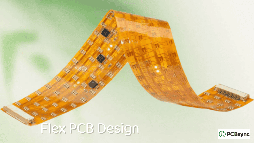
Single Layer Flex PCB: Design Guide, Applications & Cost Benefits
About eight years ago, I was tasked with redesigning a fitness tracker’s internal connections. The original design used ribbon cables and connectors that added weight, created potential failure points, and complicated assembly. Switching to a 1 layer flex PCB solved all three problems in one move. The single-sided flexible circuit replaced multiple cables, cut assembly time in half, and eliminated the connector reliability issues that plagued the first-generation product.
That project convinced me that 1 layer flex PCB technology deserves more attention from designers who default to multi-layer solutions. For many applications, single-layer flexible circuits deliver everything you need at significantly lower cost and faster turnaround. Here’s what you need to know about designing with them effectively.
A 1 layer flex PCB is a flexible printed circuit board with a single conductive copper layer on a flexible polyimide or polyester substrate. Unlike rigid PCBs built on stiff FR4 material, single-layer flex circuits can bend, fold, and conform to three-dimensional shapes while maintaining electrical connectivity.
The basic structure consists of four elements: a flexible base film (typically polyimide), a single copper layer etched with circuit traces, an adhesive layer bonding copper to substrate, and a protective coverlay on top. This simple construction makes 1 layer flex PCB the most straightforward and cost-effective flexible circuit option available.
Despite having just one conductive layer, single-layer flex circuits support a surprising range of functionality. They accommodate surface-mount components, through-hole pins, connectors, and stiffeners for localized rigidity. For applications requiring simple point-to-point connections or moderate circuit complexity, a 1 layer flex PCB often provides the optimal balance of capability and cost.
Structure and Stack-Up of Single Layer Flex PCB
Understanding the layer construction helps you specify materials correctly and anticipate manufacturing constraints.
Typical 1 Layer Flex PCB Stack-Up
Layer
Material
Typical Thickness
Function
Coverlay
Polyimide film + adhesive
12.5-50 μm
Protects copper traces
Copper
Rolled annealed (RA) or electrodeposited (ED)
9-70 μm (¼ oz to 2 oz)
Conductive traces
Adhesive
Acrylic or epoxy
12.5-25 μm
Bonds copper to substrate
Base Film
Polyimide (PI) or Polyester (PET)
12.5-125 μm
Flexible substrate
The total thickness of a 1 layer flex PCB typically ranges from 0.08mm to 0.15mm (80-150 μm), making it significantly thinner than even the thinnest rigid PCBs. This thinness contributes directly to flexibility and weight reduction.
Material Options for Single Layer Flex
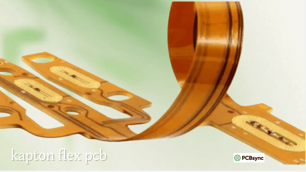
Polyimide (PI) is the industry standard for high-performance 1 layer flex PCB applications. Kapton, DuPont’s branded polyimide, offers excellent thermal stability (withstanding soldering temperatures), chemical resistance, and mechanical durability. Polyimide substrates handle dynamic flexing applications where the circuit bends repeatedly during operation.
Polyester (PET) provides a more economical alternative for less demanding applications. PET costs 20-30% less than polyimide but has lower temperature resistance (max ~105°C vs 260°C for PI). For static applications where the flex circuit bends only during installation, polyester often delivers adequate performance at reduced cost.
Copper Types: RA vs ED
Rolled Annealed (RA) copper is the preferred choice for dynamic flexing applications. The rolling process aligns the copper’s grain structure, providing superior fatigue resistance when the circuit flexes repeatedly. RA copper costs more but can withstand millions of flex cycles without cracking.
Electrodeposited (ED) copper costs less and works well for static flex applications—circuits that bend once during installation and remain stationary thereafter. ED copper’s grain structure makes it more prone to fatigue cracking under repeated flexing, limiting its use in dynamic applications.
Single-layer flexible circuits serve two primary application categories: static and dynamic.
Static Flex Applications (Flex-to-Install)
In static applications, the 1 layer flex PCB bends during installation to fit within the product enclosure but doesn’t flex during normal operation. These applications can use less expensive ED copper and polyester substrates.
Common static applications include:
LED lighting connections
Display interfaces
Battery connections in portable devices
Sensor interconnects
Point-to-point wiring replacement
Automotive interior electronics
Dynamic Flex Applications (Repeated Flexing)
Dynamic applications require the circuit to flex continuously during product operation. These demand RA copper and polyimide substrates designed for fatigue resistance.
A 1 layer flex PCB costs approximately 30-50% less than an equivalent two-layer design and 60-70% less than four-layer alternatives. For high-volume production, these savings compound significantly.
Why Single Layer Flex Costs Less
Simpler manufacturing process: Single-layer circuits require fewer processing steps—no lamination of multiple layers, no drilling and plating of vias between layers. This reduces both material costs and labor.
Faster production time: With fewer process steps, 1 layer flex PCB production times are shortest in the flex circuit category. Some manufacturers offer 24-hour turnaround for simple single-layer designs.
Higher yields: Simpler construction means fewer opportunities for manufacturing defects. Higher yields translate directly to lower per-unit costs.
Reduced material usage: One copper layer means less copper, less adhesive, and less substrate material per circuit. Material costs dominate flex PCB pricing, so this reduction matters.
Hidden Cost Savings
Beyond direct PCB costs, 1 layer flex PCB designs often reduce total system costs:
Eliminates connectors: Replacing wire harnesses with flex circuits removes connector costs and assembly labor
Simplifies testing: Fewer interconnection points mean fewer potential failure modes to test
Lowers weight: Lighter products reduce shipping costs and may improve end-product performance
Design Guidelines for 1 Layer Flex PCB
Designing effective single-layer flex circuits requires attention to flexibility requirements, trace routing, and component placement.
Trace Width and Spacing
For 1 layer flex PCB, use wider traces than you would on rigid boards. Flexible substrates move, and narrow traces are more susceptible to fatigue cracking at bend points.
Design Parameter
Recommended Minimum
Notes
Trace Width
4 mils (0.1mm)
6-8 mils preferred for dynamic flex
Trace Spacing
4 mils (0.1mm)
Larger spacing improves yield
Annular Ring
8 mils (0.2mm)
Larger rings improve reliability
Pad-to-Trace
8 mils (0.2mm)
Prevents solder bridging
Bend Radius Considerations
The minimum bend radius depends on copper thickness, substrate thickness, and whether the application is static or dynamic:
Static applications: Minimum bend radius = 6× total circuit thickness
Dynamic applications: Minimum bend radius = 12× total circuit thickness (for >1 million cycles)
For a typical 0.1mm thick 1 layer flex PCB, this means:
Static: 0.6mm minimum bend radius
Dynamic: 1.2mm minimum bend radius
Trace Routing Best Practices
Route traces perpendicular to bend lines when possible
Avoid routing traces through tight-radius bend areas
Use curved traces rather than 90-degree corners in flex zones
Maintain uniform trace width through bend areas
Don’t place vias or pads in flex zones
Component Placement
Single-layer flex circuits support surface-mount components, but placement requires careful consideration:
Place components only in rigid areas (use stiffeners if needed)
Keep components away from bend zones
Ensure adequate pad sizes for reliable solder joints
Consider component weight and its effect on flex behavior
Understanding the manufacturing process helps you design for manufacturability and set realistic expectations for cost and lead time.
Production Steps
Material preparation: Cut polyimide base film to panel size
Copper lamination: Bond copper foil to substrate using heat and pressure
Photolithography: Apply photoresist and expose circuit pattern
Etching: Remove unwanted copper to create traces
Coverlay application: Laminate protective coverlay over copper traces
Surface finish: Apply ENIG, immersion tin, or other finish to exposed pads
Profiling: Cut individual circuits from panel
Stiffener attachment: Bond stiffeners if required
Testing: Electrical testing and visual inspection
Lead Time Expectations
Order Type
Typical Lead Time
Quick-turn prototype
24-72 hours
Standard prototype
5-7 days
Small batch production
7-14 days
Volume production
14-21 days
Single-layer flex circuits have the shortest lead times among flex PCB types because they require fewer processing steps and no layer-to-layer registration.
Specifications and Capabilities
Typical 1 Layer Flex PCB Specifications
Parameter
Standard Capability
Advanced Capability
Minimum Trace Width
4 mils (0.1mm)
2 mils (0.05mm)
Minimum Spacing
4 mils (0.1mm)
2 mils (0.05mm)
Copper Thickness
½ oz – 2 oz
¼ oz – 4 oz
Total Thickness
0.08-0.15mm
0.05-0.25mm
Minimum Hole Size
8 mils (0.2mm)
4 mils (0.1mm)
Surface Finishes
ENIG, Immersion Tin, OSP
Hard Gold, Selective Gold
Coverlay Options
Yellow PI, Black PI
White PI, Clear PI
Operating Temperature
-40°C to +85°C
-55°C to +150°C
Frequently Asked Questions About 1 Layer Flex PCB
Can single-layer flex PCBs handle surface-mount components?
Yes. 1 layer flex PCB designs support SMT components when proper design guidelines are followed. Use stiffeners under component areas to provide a flat, rigid mounting surface. Ensure adequate pad sizes (typically 10-15% larger than rigid board standards) and maintain sufficient spacing between components. Most manufacturers can assemble 0402 components and larger on single-layer flex circuits.
How many flex cycles can a 1 layer flex PCB withstand?
With proper design and RA copper, single-layer flex circuits routinely withstand 1 million+ flex cycles in dynamic applications. Some designs achieve 500 million cycles. Key factors include copper type (RA required for dynamic flex), bend radius (larger is better), copper thickness (thinner flexes more easily), and trace routing (perpendicular to bend line is optimal). For static applications where flexing occurs only during installation, cycle life isn’t a concern.
What’s the difference between 1 layer flex PCB and FFC cables?
Flat Flexible Cables (FFC) are mass-produced, standardized ribbon cables with parallel conductors at fixed pitches. They’re inexpensive but limited to simple point-to-point connections. A 1 layer flex PCB is a custom-designed circuit that can include complex trace routing, branches, multiple connector interfaces, and component mounting. Use FFC for simple, standard connections; use single-layer flex for custom routing requirements.
Should I choose polyimide or polyester for my flex circuit?
Choose polyimide (PI) for applications requiring high temperature resistance (soldering, automotive, LED lighting), dynamic flexing, or long-term reliability. Choose polyester (PET) for cost-sensitive consumer applications with static flex requirements and operating temperatures below 85°C. When in doubt, polyimide provides better all-around performance and is the safer choice for most applications.
How do I reduce 1 layer flex PCB costs?
Several strategies reduce single-layer flex costs: design with standard material thicknesses rather than custom, use ED copper if your application allows static flex only, choose polyester over polyimide where temperature requirements permit, optimize panel utilization by adjusting circuit dimensions, specify standard surface finishes (ENIG or immersion tin rather than hard gold), and consolidate multiple designs on shared panels when practical.
Useful Resources for Single Layer Flex PCB Design
Design Standards
IPC-6013: Qualification and Performance Specification for Flexible/Rigid-Flexible Printed Boards
IPC-2223: Sectional Design Standard for Flexible Printed Boards
Controlled impedance requires specific stackup configurations
Mixed rigid and flex functionality is needed in one assembly
For many applications I’ve worked on over the years, 1 layer flex PCB provides the optimal solution—delivering the flexibility benefits designers need without the complexity and cost of multi-layer alternatives. Start with single-layer when your routing allows it; you can always add layers if the design demands it.
The fitness tracker redesign I mentioned at the start? It’s been in production for six years now, still using that original single-layer flex design. Sometimes the simplest solution really is the best one.
Inquire: Call 0086-755-23203480, or reach out via the form below/your sales contact to discuss our design, manufacturing, and assembly capabilities.
Quote: Email your PCB files to Sales@pcbsync.com (Preferred for large files) or submit online. We will contact you promptly. Please ensure your email is correct.
Notes: For PCB fabrication, we require PCB design file in Gerber RS-274X format (most preferred), *.PCB/DDB (Protel, inform your program version) format or *.BRD (Eagle) format. For PCB assembly, we require PCB design file in above mentioned format, drilling file and BOM. Click to download BOM template To avoid file missing, please include all files into one folder and compress it into .zip or .rar format.


