Inquire: Call 0086-755-23203480, or reach out via the form below/your sales contact to discuss our design, manufacturing, and assembly capabilities.
Quote: Email your PCB files to Sales@pcbsync.com (Preferred for large files) or submit online. We will contact you promptly. Please ensure your email is correct.
Notes: For PCB fabrication, we require PCB design file in Gerber RS-274X format (most preferred), *.PCB/DDB (Protel, inform your program version) format or *.BRD (Eagle) format. For PCB assembly, we require PCB design file in above mentioned format, drilling file and BOM. Click to download BOM template To avoid file missing, please include all files into one folder and compress it into .zip or .rar format.
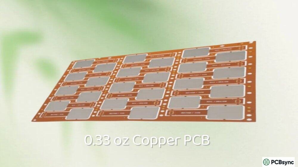
When you’re designing the next smartphone, wearable device, or any HDI application where every micron matters, 1/3oz Copper PCB becomes your best friend. I’ve spent years working with ultra-thin copper specifications, and understanding when to use 12-micron copper can make or break your miniaturization goals.
This guide covers everything you need to know about 1/3oz copper PCB technology—from basic specifications to advanced design guidelines that will help you achieve fine-pitch routing without compromising reliability.
1/3oz Copper PCB refers to a printed circuit board manufactured with copper foil weighing one-third of an ounce per square foot. When this copper is spread evenly across that area, it produces a thickness of approximately 12 micrometers (0.47 mils).
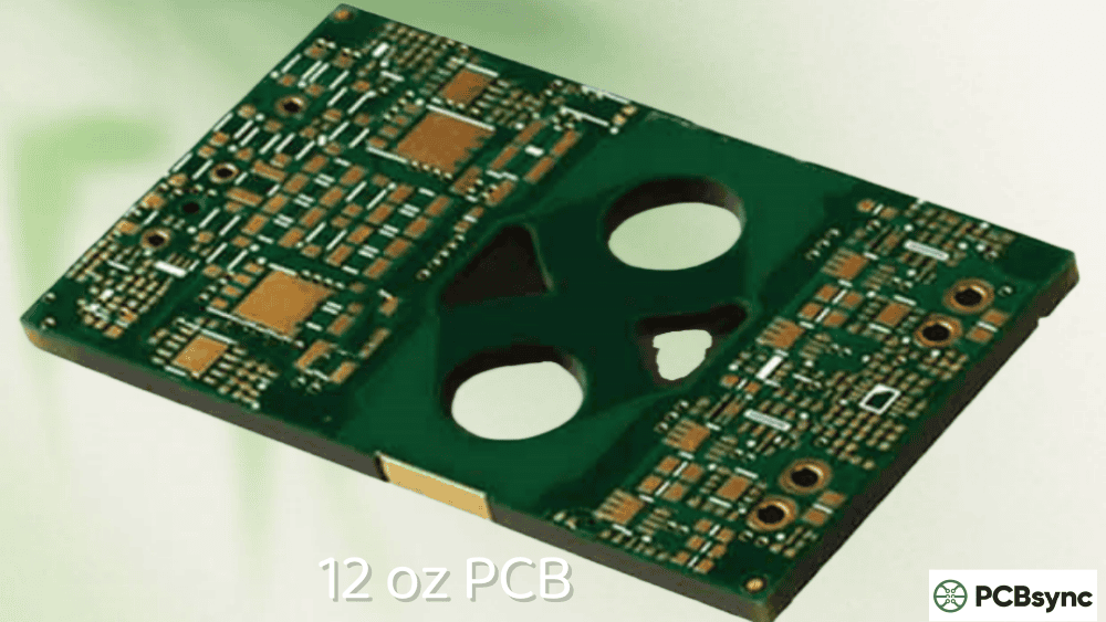
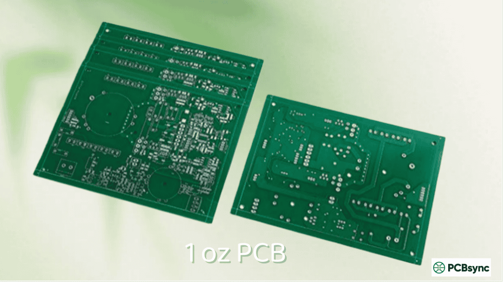
To put this in perspective: standard PCBs use 1oz copper at 35μm thickness. A 1/3oz copper layer is literally three times thinner than the industry standard—and that difference opens up possibilities that simply don’t exist with heavier copper weights.
Understanding Copper Weight Measurements
The PCB industry measures copper thickness by weight rather than direct thickness for historical reasons. Here’s how 1/3oz compares to other common copper weights:
The formula behind this measurement: when 1/3 ounce (approximately 9.45 grams) of copper covers one square foot uniformly, it results in a 12μm thick layer.
The primary driver for selecting 1/3oz copper PCB is achieving finer feature sizes than possible with standard copper weights. When you need traces and spaces below 75 microns (3 mils), thin copper isn’t optional—it’s mandatory.
Enabling Ultra-Fine Line Technology
Copper etching is a subtractive process. The thicker your starting copper, the more lateral etching occurs as chemicals work down to the substrate. This lateral etching—called undercut—directly limits how narrow your traces can be.
With 1/3oz copper, you can reliably achieve:
Trace widths down to 50μm (2 mils)
Trace spacing down to 50μm (2 mils)
75μm (3 mil) traces with tight process control
Fine-pitch BGA breakout at 0.4mm pitch and below
Try achieving those specifications with 1oz copper, and you’ll face yield issues, inconsistent etching, and potential shorts from insufficient clearance.
Supporting HDI and Microvia Technology
High-Density Interconnect (HDI) PCBs rely on thin copper for several reasons:
Microvia formation: Laser-drilled microvias work best with thin copper because the copper layer must be ablated before reaching the dielectric. Thinner copper means faster, cleaner drilling and smaller capture pads.
Via-in-pad designs: When placing microvias directly in component pads, the copper thickness affects the overall pad height after filling and plating. Thinner base copper produces flatter pads for reliable solder joints.
Sequential lamination: Build-up layers in HDI construction use Resin Coated Copper (RCC) foils, which are specifically designed with ultra-thin copper (often 1/3oz or thinner) for fine-line capability.
Reducing Overall Board Thickness
For ultra-thin PCB designs—particularly in smartphones, wearables, and medical implants—every micron counts. Using 1/3oz copper instead of 1oz on all layers can reduce total stack-up thickness by 46μm on a 4-layer board. That might sound trivial, but in applications targeting sub-0.4mm total thickness, it’s significant.
1/3oz Copper PCB Specifications and Performance
Understanding the electrical and mechanical characteristics of 1/3oz copper helps you design within its capabilities.
Electrical Properties Comparison
Parameter
1/3oz (12μm)
1/2oz (18μm)
1oz (35μm)
Sheet Resistance
~1.4 mΩ/sq
~0.95 mΩ/sq
~0.49 mΩ/sq
Current Capacity (10mil trace, 10°C rise)
~0.5A
~0.7A
~1.2A
Skin Depth @ 1GHz
2.1 μm
2.1 μm
2.1 μm
Minimum Trace Width
2 mil (50μm)
3 mil (75μm)
4 mil (100μm)
Minimum Spacing
2 mil (50μm)
3 mil (75μm)
4 mil (100μm)
The key takeaway: 1/3oz copper has approximately three times the resistance per unit length compared to 1oz copper. For signal traces carrying milliamp-level currents, this is rarely a problem. For power distribution, you’ll need to compensate with wider traces.
High-Frequency Performance Considerations
At RF and microwave frequencies, the skin effect concentrates current flow on the conductor surface. At 1 GHz, copper’s skin depth is only about 2.1 micrometers. At 10 GHz, it drops to roughly 0.66 micrometers.
This means for high-frequency applications, 1/3oz copper (12μm) provides more than adequate conductor depth—the signals aren’t penetrating beyond the first few microns anyway. In fact, thinner copper with controlled surface roughness often outperforms thicker copper at high frequencies because surface quality becomes more critical than bulk thickness.
For high-frequency 1/3oz copper PCB designs:
Surface roughness matters more than copper weight
Consider low-profile or ultra-low-profile (ULP) copper foils
Rolled annealed copper provides smoother surfaces than electrodeposited copper
Applications for 1/3oz Copper PCB Technology
The applications driving demand for 1/3oz copper PCB share common requirements: miniaturization, high density, and fine-pitch components.
Smartphones and Mobile Devices
Modern smartphones pack incredible functionality into remarkably thin form factors. The main logic boards in flagship phones routinely use 1/3oz copper on HDI layers to achieve:
0.35mm pitch BGA routing for application processors
Any-layer microvia structures for maximum routing density
8-12 layer boards in under 1mm total thickness
Fine-pitch connections to camera modules, displays, and RF front-ends
Wearable Electronics
Smartwatches, fitness trackers, and wireless earbuds face extreme space constraints. These devices benefit from 1/3oz copper PCB technology through:
Ultra-thin rigid-flex construction
Miniaturized sensor integration
Compact battery management circuits
High-density interconnects in curved form factors
Medical Devices and Implants
Medical electronics—particularly implantable devices—demand the smallest possible footprint with absolute reliability. Applications include:
Cochlear implants
Pacemaker controllers
Neural interfaces
Diagnostic imaging components
These designs often combine 1/3oz copper with specialized biocompatible materials and hermetic packaging.
Package Substrates and Interposers
The semiconductor packaging industry uses even thinner copper than typical PCBs, but 1/3oz serves as a bridge between standard PCB technology and advanced packaging. Applications include:
Flip-chip BGA substrates
System-in-Package (SiP) substrates
High-bandwidth memory (HBM) interposers
Advanced chip-scale packaging
Consumer Electronics
Beyond smartphones, many consumer devices benefit from 1/3oz copper capability:
Tablets and laptops (main boards and display interconnects)
Gaming controllers with haptic feedback
True wireless stereo (TWS) earbuds
Action cameras and drones
Design Guidelines for 1/3oz Copper PCB
Designing with ultra-thin copper requires adjustments to your standard PCB design practices.
Trace Width and Current Capacity
The reduced cross-sectional area of 1/3oz copper directly impacts current-carrying capacity. Use these guidelines:
Current Required
1/3oz Trace Width
1oz Trace Width
Reduction Possible
0.5A
10 mil (0.25mm)
5 mil (0.125mm)
Use 1oz for power
0.3A
6 mil (0.15mm)
3 mil (0.075mm)
1/3oz acceptable
0.1A
3 mil (0.075mm)
2 mil (0.05mm)
1/3oz preferred
Signal only
2 mil (0.05mm)
2 mil (0.05mm)
1/3oz enables this
For designs mixing signal routing with power distribution, consider using different copper weights on different layers—1/3oz for signal layers where fine lines are needed, and 1oz or heavier for power planes.
Impedance Control
Thinner copper affects controlled impedance calculations. For a given target impedance:
Trace widths will be slightly narrower with 1/3oz copper
The effect is relatively small for microstrip configurations
Stripline impedance is less sensitive to copper thickness variations
Work with your fabricator early to obtain accurate impedance modeling that accounts for the specific copper weight and dielectric materials in your stack-up.
Via and Pad Design
When using 1/3oz copper PCB with microvias:
Maintain aspect ratios below 1:1 (preferably 0.75:1) for reliable plating
Size capture pads appropriately for your fabricator’s registration capability
Consider via-in-pad with filled and plated vias for maximum density
Account for copper thickness when calculating total pad height after plating
The formula for microvia diameter: Microvia Diameter = (Dielectric Thickness + Copper Thickness) / Aspect Ratio
Thermal Management
Thin copper conducts heat less effectively than thicker copper. Mitigation strategies include:
Thermal vias connecting to internal copper planes
Exposed copper pads or thermal coins for high-power components
Wider traces for power paths to reduce I²R heating
Strategic use of heavier copper on selected layers
Cost Analysis: 1/3oz Copper PCB vs Standard Copper
Understanding cost drivers helps you make informed decisions about when thin copper is worth the premium.
Cost Factor
Impact
Notes
Material Cost
Moderate increase
Specialty foil pricing
Processing Cost
Higher
Tighter controls required
Yield
Lower
More sensitivity to defects
Lead Time
Longer
Material availability
Overall Premium
15-30% typical
Versus standard 1oz copper
The cost premium varies significantly based on:
Layer count and complexity
Required line width/spacing
Fabricator capabilities and experience
Order volume and delivery requirements
For high-volume consumer electronics, the per-unit cost premium becomes acceptable given the miniaturization benefits. For low-volume prototypes, consider whether 1/3oz copper is truly necessary or if you can achieve your goals with 1/2oz copper at lower cost.
Useful Resources and Technical References
IPC Standards for Thin Copper PCB Design
IPC-2221: Generic Standard on Printed Board Design (includes current capacity guidelines)
What is the actual thickness of 1/3oz copper in microns?
1/3oz copper has a thickness of approximately 12 micrometers (μm), which equals 0.47 mils or 0.012mm. This measurement represents the copper foil before any plating processes. After panel plating and pattern plating, outer layer copper thickness typically increases by 15-25μm, so finished outer layer thickness may be 27-37μm even when starting with 1/3oz base copper.
Can 1/3oz copper PCB handle lead-free soldering temperatures?
Yes, 1/3oz copper PCB is fully compatible with lead-free soldering processes. The copper thickness doesn’t affect thermal compatibility—that’s determined by the laminate material’s Tg and Td values. However, the thinner copper does mean slightly less thermal mass, so heat-up rates during reflow may be marginally faster. This rarely causes practical issues but should be considered for thermally sensitive components.
What is the minimum trace width achievable with 1/3oz copper?
With 1/3oz copper, most fabricators can reliably achieve 2-3 mil (50-75μm) trace widths and spaces using subtractive etching processes. For even finer features (below 2 mils), advanced techniques like modified Semi-Additive Process (mSAP) or Semi-Additive Process (SAP) are required, which use ultra-thin copper of 5μm or less as a seed layer. Standard 1/3oz copper with conventional processing typically bottoms out around 2 mil traces.
How does 1/3oz copper affect PCB impedance calculations?
Copper thickness is one variable in impedance calculations, but its effect is relatively small compared to dielectric thickness and trace width. For microstrip configurations, changing from 1oz to 1/3oz copper might require a trace width adjustment of 5-10% to maintain the same impedance. The more significant impact is that 1/3oz copper enables narrower traces that wouldn’t be manufacturable with thicker copper, allowing higher-impedance designs (like 100Ω differential pairs) at tighter pitches.
When should I use 1/3oz copper versus 1/2oz copper?
Choose 1/3oz copper when your design requires trace widths below 3 mils (75μm), you’re working with HDI technology requiring build-up layers with RCC, or absolute minimum board thickness is critical. Choose 1/2oz copper (18μm) when you need traces in the 3-4 mil range, want slightly better current capacity than 1/3oz, or need a balance between fine-line capability and manufacturability. The 1/2oz option often provides the best cost-performance balance for designs that don’t push ultra-fine-line limits.
Final Thoughts
1/3oz Copper PCB technology enables the miniaturization that modern electronics demand. From smartphones to medical implants, ultra-thin copper makes possible the fine-pitch routing and high-density interconnects that define cutting-edge products.
The trade-offs are real: reduced current capacity, manufacturing sensitivity, and higher costs compared to standard copper weights. But when your design requires traces below 3 mils or HDI structures with stacked microvias, 1/3oz copper isn’t just an option—it’s a necessity.
Work closely with your fabricator early in the design process. Their capabilities and material availability will guide your design rules. Not every shop can deliver 2 mil traces on 1/3oz copper reliably, but those that specialize in HDI manufacturing handle this technology daily.
The trend toward thinner copper continues. As consumer electronics, automotive systems, and medical devices demand ever-smaller form factors, 1/3oz copper—and even thinner options—will become increasingly common. Understanding this technology now positions you for the designs of tomorrow.
Inquire: Call 0086-755-23203480, or reach out via the form below/your sales contact to discuss our design, manufacturing, and assembly capabilities.
Quote: Email your PCB files to Sales@pcbsync.com (Preferred for large files) or submit online. We will contact you promptly. Please ensure your email is correct.
Notes: For PCB fabrication, we require PCB design file in Gerber RS-274X format (most preferred), *.PCB/DDB (Protel, inform your program version) format or *.BRD (Eagle) format. For PCB assembly, we require PCB design file in above mentioned format, drilling file and BOM. Click to download BOM template To avoid file missing, please include all files into one folder and compress it into .zip or .rar format.


